Hardware Interface Description
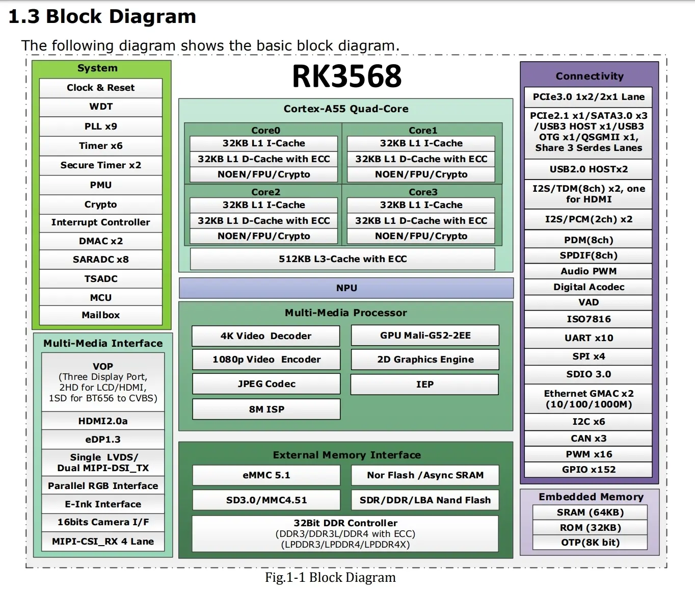
Chip block diagram
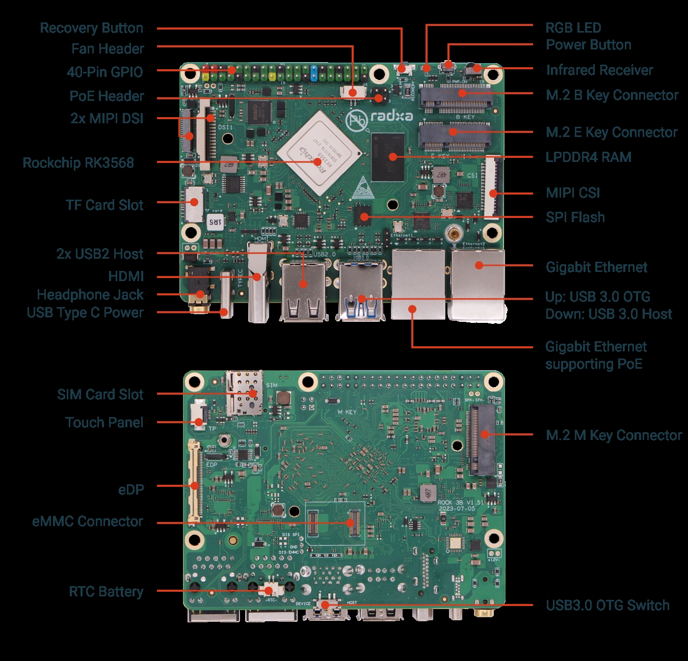
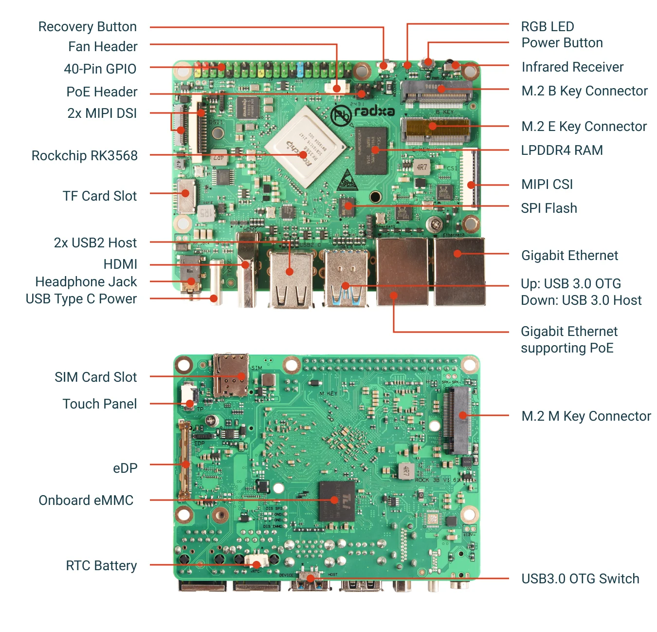
Physical photographs
- ROCK 3B
- ROCK 3B+
Interface details
40-PIN GPIO Header
GPIO Voltage
| Type | Voltage | Tolerance |
|---|---|---|
| GPIO | 3.3V | 3.63V |
| ADC | 1.8V | 1.98V |
GPIO Pinout
ROCK 3B provides a 40 pin GPIO socket that is compatible with most sensor applications on the market.
Actual compatibility is subject to actual use.
- v1.1
| GPIO number | Function4 | Function3 | Function2 | Function1 | Pin# | Pin# | Function1 | Function2 | Function3 | Function4 | GPIO number |
|---|---|---|---|---|---|---|---|---|---|---|---|
| +3.3V | 1 | 2 | +5.0V | ||||||||
| 32 | CAN1_RX_M0 | UART3_RX_M0 | I2C3_SDA_M0 | GPIO1_A0 | 3 | 4 | +5.0V | ||||
| 33 | CAN1_TX_M0 | UART3_TX_M0 | I2C3_SCL_M0 | GPIO1_A1 | 5 | 6 | GND | ||||
| 13 | PWM1_M1 | I2C2_SCL_M0 | GPIO0_B5 | 7 | 8 | GPIO0_D1 | UART2_TX_M0 | 25 | |||
| GND | 9 | 10 | GPIO0_D0 | UART2_RX_M0 | 24 | ||||||
| 116 | UART7_TX_M1 | PWM14_M0 | GPIO3_C4 | 11 | 12 | GPIO3_A3 | 99 | ||||
| 117 | UART7_RX_M1 | PWM15_IR_M0 | 13 | 14 | GND | ||||||
| 16 | UART0_RX | PWM1_M0 | GPIO0_C0 | 15 | 16 | GPIO0_B6 | I2C2_SDA_M0 | PWM2_M1 | 14 | ||
| +3.3V | 17 | 18 | GPIO3_B2 | UART4_TX_M1 | PWM9_M0 | 106 | |||||
| 146 | CAN1_TX_M1 | SPI3_MOSI_M1 | PWM15_IR_M1 | GPIO4_C3 | 19 | 20 | GND | ||||
| 149 | UART9_TX_M1 | SPI3_MISO_M1 | PWM12_M1 | GPIO4_C5 | 21 | 22 | GPIO0_C1 | PWM2_M0 | UART0_TX | 17 | |
| 147 | CAN1_RX_M1 | SPI3_CLK_M1 | PWM14_M1 | GPIO4_C2 | 23 | 24 | GPIO4_C6 | PWM13_M1 | SPI3_CS0_M1 | UART9_RX_M1 | 150 |
| GND | 25 | 26 | GPIO4_D1 | SPI3_CS1_M1 | 153 | ||||||
| 12 | USB_DP | CAN0_RX_M0 | I2C1_SDA | GPIO0_B4 | 27 | 28 | GPIO0_B3 | I2C1_SCL | CAN0_TX_M0 | USB_DM | 11 |
| 95 | GPIO2_D7 | 29 | 30 | GND | |||||||
| 96 | GPIO3_A0 | 31 | 32 | GPIO3_C2 | UART5_TX_M1 | 114 | |||||
| 115 | UART5_RX_M1 | SPI1_CLK_M1 | GPIO3_C3 | 33 | 34 | GND | |||||
| 100 | GPIO3_A4 | 35 | 36 | GPIO3_A2 | 98 | ||||||
| SARADC_VIN5 | 37 | 38 | GPIO3_A6 | 102 | |||||||
| GND | 39 | 40 | GPIO3_A5 | 101 |
-
Addition to the 40-pin Expansion Block for V1.1 Hardware Versions
- The pins marked in orange are used for debug console.
- PWM: x7, PWM1 / PWM2 / PWM9 / PWM12 / PWM13 / PWM14 / PWM15
- SPI: x1, SPI3
- I2C: x3, I2C1 / I2C2 / I2C3
- UART: x6, UART0 / UART2 /UART3 / UART5 / UART7 / UART9
- ADC: x1, SARADC_VIN5
- CAN: x2, CAN0 / CAN1
USB Function Configuration on 40-Pin
On the ROCK 3B's 40-Pin interface, the following pins can be configured for USB 2.0:
- USB3_DM: Pin number 28, resistor location R90538.
- USB3_DP: Pin number 27, resistor location R90536.
By default, Pin-27 can be configured in software for functions such as GPIO0_B4 (see 40-Pin Pinout), while the USB3_DP signal is not activated on the hardware. Pin-28 can be configured in software for functions such as GPIO0_B3 (see 40-Pin Pinout), and the USB3_DM signal is also not activated on the hardware. To change these pins to USB functions, please follow the steps below to modify the reserved resistors:
- Remove the 0-ohm resistors at R90535 and R90537.
- Solder 0-ohm resistors at R90536 and R90538.
The schematic and resistor locations can be viewed and downloaded from the hardware documentation.Hardware Documentation Download
This procedure requires soldering skills, and it is recommended that it be performed by an experienced technician.
eMMC
- ROCK 3B
- ROCK 3B+
ROCK 3B uses an onboard eMMC connector to attach an external eMMC module.
| Pin | Name | Pin | Name |
|---|---|---|---|
| 1 | GND | 2 | eMMC_D5 |
| 3 | GND | 4 | eMMC_D4 |
| 5 | GND | 6 | eMMC_D0 |
| 7 | GND | 8 | eMMC_CLKOUT |
| 9 | GND | 10 | eMMC_D3 |
| 11 | GND | 12 | eMMC_RSTn |
| 13 | GND | 14 | GND |
| 15 | 16 | GND | |
| 17 | GND | 18 | GND |
| 19 | GND | 20 | VCC18_EMMC |
| 21 | VCC18_EMMC | 22 | VCCIO_FLASH |
| 23 | VCCIO_FLASH | 24 | GND |
| 25 | eMMC_CMD | 26 | GND |
| 27 | eMMC_D2 | 28 | GND |
| 29 | eMMC_D1 | 30 | GND |
| 31 | eMMC_D7 | 32 | GND |
| 33 | eMMC_D6 | 34 | GND |
| 35 | GND | 36 | GND |
| 37 | GND | 38 | GND |
| 39 | GND | 40 | GND |
| 41 | GND | 42 | GND |
| 43 | GND | 44 | GND |
| 45 | GND | 46 | GND |
| 47 | GND | 48 | GND |
| 49 | GND | 50 | GND |
| 51 | GND | 52 | GND |
| 53 | GND | 54 | GND |
| 55 | GND | 56 | GND |
| 57 | GND | 58 | GND |
| 59 | GND | 60 | GND |
| 61 | GND | 62 | GND |
| 63 | GND | 64 | GND |
ROCK 3B+ uses an onboard eMMC module and does not require an external eMMC connector.
SPI Flash
The SPI Flash is onboard on both ROCK 3B and ROCK 3B+; no external connector is required.
FAN
| Pin | Name | Pin | Name |
|---|---|---|---|
| 1 | GPIO3_B1/PWM8 | 2 | VCC5V0_SYS |
| 3 | GND | 4 | GND |
HDMI
| Pin | Name | Pin | Name |
|---|---|---|---|
| 1 | HDMI_TX2P_PORT | 2 | GND |
| 3 | HDMI_TX2N_PORT | 4 | HDMI_TX1P_PORT |
| 5 | GND | 6 | HDMI_TX1N_PORT |
| 7 | HDMI_TX0P_PORT | 8 | GND |
| 9 | HDMI_TX0N_PORT | 10 | HDMI_TXCLKP_PORT |
| 11 | GND | 12 | HDMI_TXCLKN_PORT |
| 13 | HDMI_TX_CEC_PORT | 14 | |
| 15 | HDMI_TXDDC_SCL_PORT | 16 | HDMI_TXDDC_SDA_PORT |
| 17 | GND | 18 | VCC5V_HDMI_TX |
| 19 | HDMI_TX_HPD_PORT | 20 | GND |
| 21 | GND | 22 | |
| 23 | GND |
microSD Card
| Pin | Name | Pin | Name |
|---|---|---|---|
| 1 | SDMMC0_D2/ARMJTAG_TCK | 2 | SDMMC0_D3/ARMJTAG_TMS |
| 3 | SDMMC0_CMD | VCC3V3_SD | |
| 5 | SDMMC0_CLK | GND | |
| 7 | SDMMC0_D0 | SDMMC0_D1 | |
| 9 | SDMMC0_DET_L |
MIPI
- MIPI DSI
| Pin | Name | Pin | Name |
|---|---|---|---|
| 1 | LCD_VCC | 2 | LCD_VCC |
| 3 | GPIO4_C0 | 4 | GPIO2-D3 |
| 5 | 6 | GND | |
| 7 | MIPI_DSI_TX0_D0N/LVDS_TX0_D0N | 8 | MIPI_DSI_TX0_D0P/LVDS_TX0_D0P |
| 9 | 10 | MIPI_DSI_TX0_D1N/LVDS_TX0_D1N | |
| 11 | MIPI_DSI_TX0_D1P/LVDS_TX0_D1P | 12 | GND |
| 13 | MIPI_DSI_TX0_CLKN/LVDS_TX0_CLKN | 14 | MIPI_DSI_TX0_CLKP/LVDS_TX0_CLKP |
| 15 | GND | 16 | MIPI_DSI_TX0_D2N/LVDS_TX0_D2N |
| 17 | MIPI_DSI_TX0_D2P/LVDS_TX0_D2P | 18 | GND |
| 19 | MIPI_DSI_TX0_D3N/LVDS_TX0_D3N | 20 | MIPI_DSI_TX0_D3P/LVDS_TX0_D3P |
| 21 | GND | 22 | GND |
| 23 | GPIO3_C5 | 24 | VCC3V3_SYS |
| 25 | GPIO3_C4 | 26 | I2C2_SDA |
| 27 | I2C2_SCL | 28 | GND |
| 29 | GND | 30 | LCD_VCC |
| 31 | LCD_VCC | 32 | GND |
| 33 | GND | 34 | VCC_LEDK |
| 35 | VCC_LEDK | 36 | |
| 37 | 38 | VCC_LEDA | |
| 39 | VCC_LEDA | 40 | GND |
| 41 | GND |
- MIPI CSI
| Pin | Name | Pin | Name |
|---|---|---|---|
| 1 | GND | 2 | MIPI_CSI_RX_D0N |
| 3 | MIPI_CSI_RX_D0P | 4 | GND |
| 5 | MIPI_CSI_RX_D1N | 6 | MIPI_CSI_RX_D1P |
| 7 | GND | 8 | MIPI_CSI_RX_CLK0N |
| 9 | MIPI_CSI_RX_CLK0P | 10 | GND |
| 11 | CAMERAB_PDN_L_GPIO4_D2 | 12 | REFCLK_OUT |
| 13 | I2C5_SCL_M0 | 14 | I2C5_SDA_M0 |
| 15 | VCC_CAM | 16 | |
| 17 |
SIM Card Slot
| Pin | Name | Pin | Name |
|---|---|---|---|
| C1 | GND | 1 | GND |
| C2 | SIM1_RESET | 2 | GND |
| C3 | SIM1_CLK | 3 | GND |
| C5 | GND | 4 | GND |
| C6 | GND | 5 | GND |
| C7 | SIM1_DATA | 6 | GND |
| CD | SIM1_DET | 7 | GND |
| CD- | GND | 8 | GND |
| 9 | GND | ||
| 10 | GND |
USB
- USB 2.0
| Pin | Name | Pin | Name |
|---|---|---|---|
| 1 | VCC5V0_USB_HOST2 | 2 | USB2_HOST2DM |
| 3 | USB2_HOST2DP | 4 | GND |
| 5 | VCC5V0_USB_HOST2 | 6 | USB2_HOST3DM |
| 7 | USB2_HOST3DP | 8 | |
| 9 | GND | 10 | GND |
| 11 | GND | 12 | GND |
- USB 3.0
| Pin | Name | Pin | Name |
|---|---|---|---|
| 1 | VCC5V0_USB_OTG0 | 2 | USB3_OTG0DM |
| 3 | USB3_OTG0DP | 4 | GND |
| 5 | USB3_OTG0SSRXN | 6 | USB3_OTG0SSRXP |
| 7 | GND | 8 | USB3_OTG0SSTXN |
| 9 | USB3_OTG0SSTXP | 10 | GND |
| 11 | GND | 12 | VCC5V0_USB_HOST1 |
| 13 | USB3_HOST1DM | 14 | USB3_HOST1DP |
| 15 | GND | 16 | USB3_HOST1SSRXN |
| 17 | USB3_HOST1SSRXP | 18 | GND |
| 19 | USB3_HOST1SSTXN | 20 | USB3_HOST1SSTXP |
| 21 | GND | 22 | GND |
PCIe
- B Key
| Pin | Name | Pin | Name |
|---|---|---|---|
| 1 | 2 | VCC3V3_PCIE30X1 | |
| 3 | GND | 4 | VCC3V3_PCIE30X1 |
| 5 | GND | 6 | 4G_PWREN_H_GPIO0_C6 |
| 7 | USB2_HOST3_DP | 8 | 4G_DISABLE_GPIO1_B0 |
| 9 | USB2_HOST3_DM | 10 | |
| 11 | GND | ||
| 20 | |||
| 21 | GND | 22 | |
| 23 | 4G_WAKE_ON_HOST | 24 | |
| 25 | 26 | GPIO2-D2 | |
| 27 | GND | 28 | |
| 29 | 30 | SIM1_RESET | |
| 31 | 32 | SIM1_CLK | |
| 33 | GND | 34 | SIM1_DATA |
| 35 | 36 | SIM1_PWR | |
| 37 | 38 | ||
| 39 | GND | 40 | |
| 41 | 42 | ||
| 43 | 44 | ||
| 45 | GND | 46 | |
| 47 | 48 | ||
| 49 | 50 | ||
| 51 | GND | 52 | |
| 53 | 54 | ||
| 55 | 56 | ||
| 57 | GND | 58 | |
| 59 | 60 | ||
| 61 | 62 | ||
| 63 | 64 | ||
| 65 | 66 | SIM1_DET | |
| 67 | 4G_RESET | 68 | |
| 69 | GND | 70 | VCC3V3_PCIE30X1 |
| 71 | GND | 72 | VCC3V3_PCIE30X1 |
| 73 | GND | 74 | VCC3V3_PCIE30X1 |
| 75 | GND | 76 | |
| 77 | GND | 78 |
- E Key
| Pin | Name | Pin | Name |
|---|---|---|---|
| 1 | GND | 2 | VCC3V3_WF |
| 3 | USB4_Dp | 4 | VCC3V3_WF |
| 5 | USB4_DM | 6 | |
| 7 | GND | 8 | |
| 9 | SDMMC2_CLK_M0 | 10 | |
| 11 | WIFI1T1R_CMD | 12 | |
| 13 | WIFI1T1R_D0 | 14 | |
| 15 | WIFI1T1R_D1 | 16 | |
| 17 | WIFI1T1R_D2 | 18 | |
| 19 | WIFI1T1R_D3 | 20 | HOST_WAKE_BT_H_GPIO4_B5 |
| 21 | WIFI_WAKE_HOST_H_GPIO3_D5 | 22 | UART8_RX_M0 |
| 23 | |||
| 32 | UART8_CTS_M0 | ||
| 33 | 34 | UART8_RTS_M0 | |
| 35 | SATA2_TXP | 36 | |
| 37 | SATA2_TXN | 38 | |
| 39 | 40 | ||
| 41 | SATA2_RXP | 42 | |
| 43 | SATA2_RXN | 44 | |
| 45 | GND | 46 | |
| 47 | PCIE20_CLKP | 48 | |
| 49 | PCIE20_CLKN | 50 | WIFIBT_32KIN_1T1R |
| 51 | GND | 52 | PCIE30X1_PERSTn_3V3_L |
| 53 | PCIE20-CLKREQN | 54 | BT_WAKE_HOST_H_GPIO4_B4 |
| 55 | PCIE20-WAKEN | 56 | |
| 57 | GND | 58 | I2C8_SDA |
| 59 | 60 | I2C8_SCL | |
| 61 | 62 | ||
| 63 | GND | 64 | |
| 65 | 66 | ||
| 67 | 68 | ||
| 69 | GND | 70 | BT_WAKE_HOST_H_GPIO4_B4 |
| 71 | 72 | VCC3V3_WF | |
| 73 | 74 | VCC3V3_WF | |
| 75 | GND | 76 | GND |
| 77 | GND | 78 | |
| 79 |
- M Key
| Pin | Name | Pin | Name |
|---|---|---|---|
| 1 | GND | 2 | VCC3V3_SYS2 |
| 3 | GND | 4 | VCC3V3_SYS2 |
| 5 | 6 | ||
| 7 | 8 | ||
| 9 | GND | 10 | |
| 11 | 12 | VCC3V3_SYS2 | |
| 13 | 14 | VCC3V3_SYS2 | |
| 15 | GND | 16 | VCC3V3_SYS2 |
| 17 | 18 | VCC3V3_SYS2 | |
| 19 | 20 | ||
| 21 | GND | 22 | |
| 23 | 24 | ||
| 25 | 26 | ||
| 27 | GND | 28 | |
| 29 | PCIE30_RX1N | 30 | |
| 31 | PCIE30_RX1P | 32 | |
| 33 | GND | 34 | |
| 35 | PCIE30_TX1N | 36 | |
| 37 | PCIE30_TX1P | 38 | |
| 39 | GND | 40 | |
| 41 | PCIE30_RX0N | 42 | |
| 43 | PCIE30_RX0P | 44 | |
| 45 | GND | 46 | |
| 47 | PCIE30_TX0N | 48 | |
| 49 | PCIE30_TX0P | 50 | PCIE30X2_LANE0_PERSTn_3V3_L |
| 51 | GND | 52 | PCIE30X2_LANE0_CLKREQn_3V3_L |
| 53 | PCIE30_REFCLKN_CON | 54 | PCIE30X2_LANE0_WAKEn_3V3_L |
| 55 | PCIE30_REFCLKP_CON | 56 | |
| 57 | GND | 58 | |
| 67 | 68 | ||
| 69 | 70 | VCC3V3_SYS2 | |
| 71 | GND | 72 | VCC3V3_SYS2 |
| 73 | GND | 74 | VCC3V3_SYS2 |
| 75 | GND |