Hardware Interface Specifications
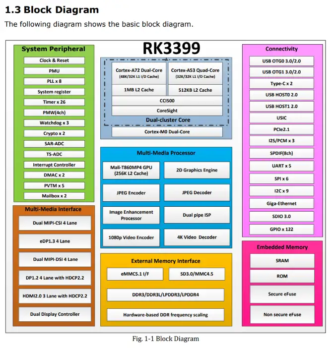
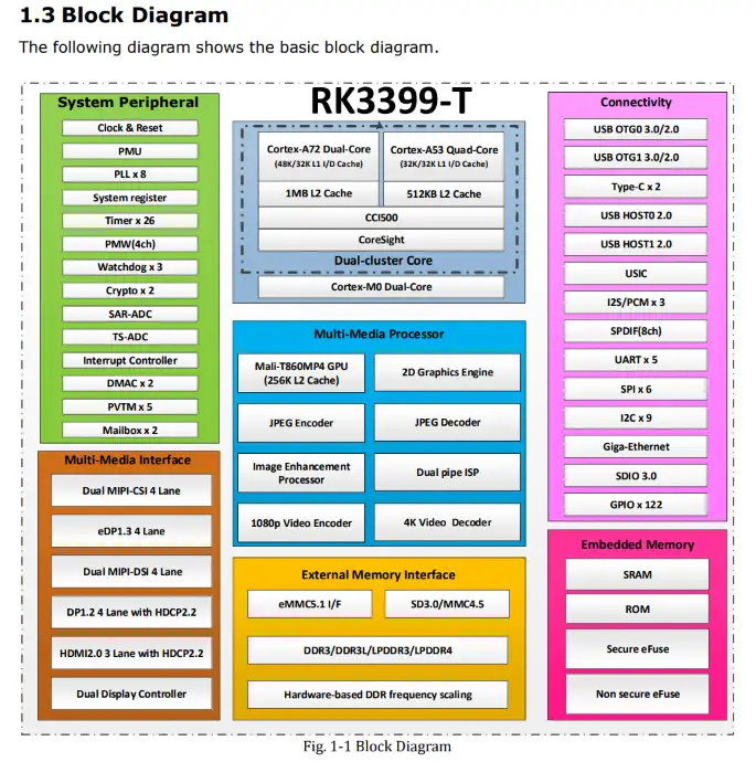
Chip Block Diagram
- Rockchip RK3399
- Rockchip RK3399-T
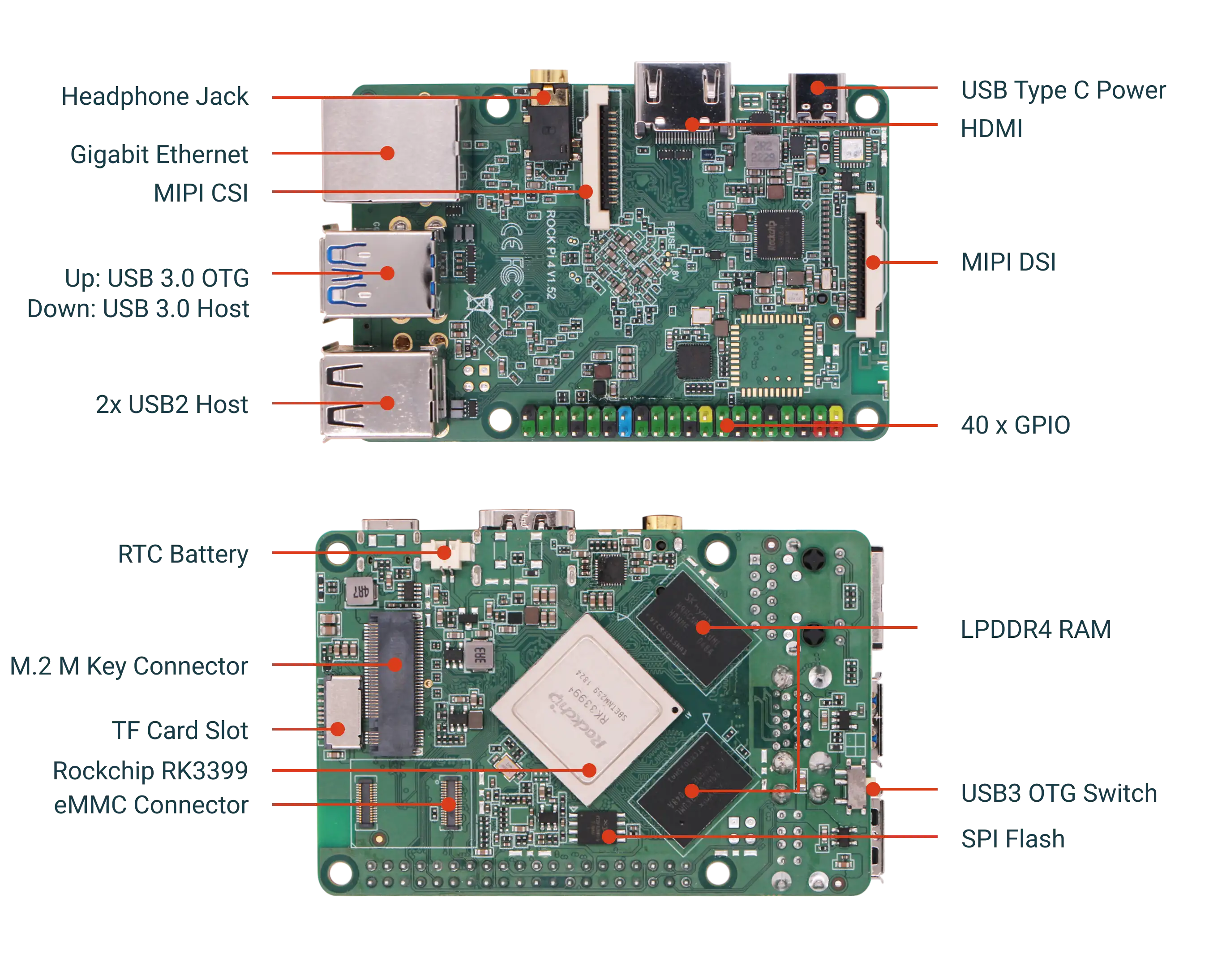
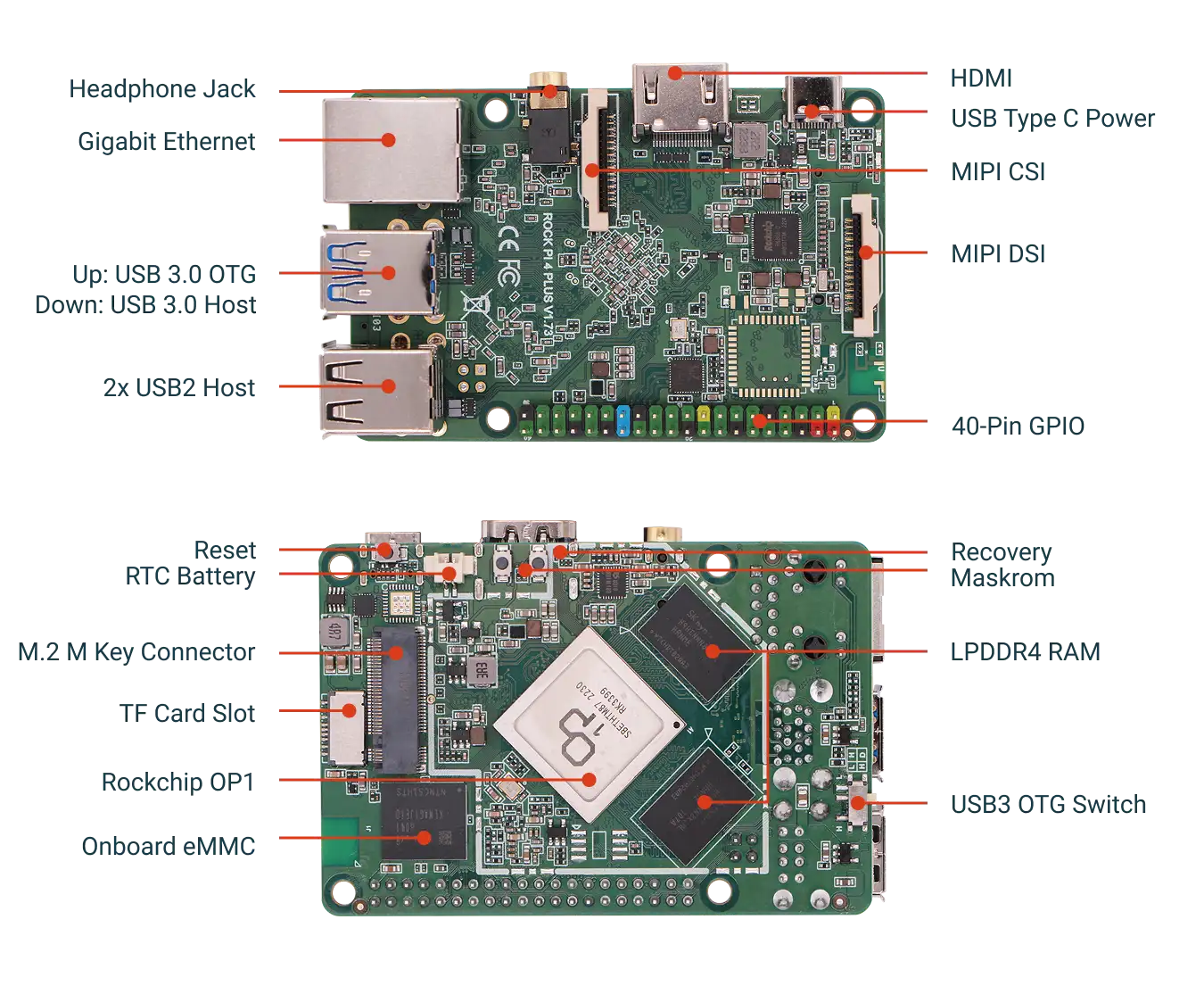
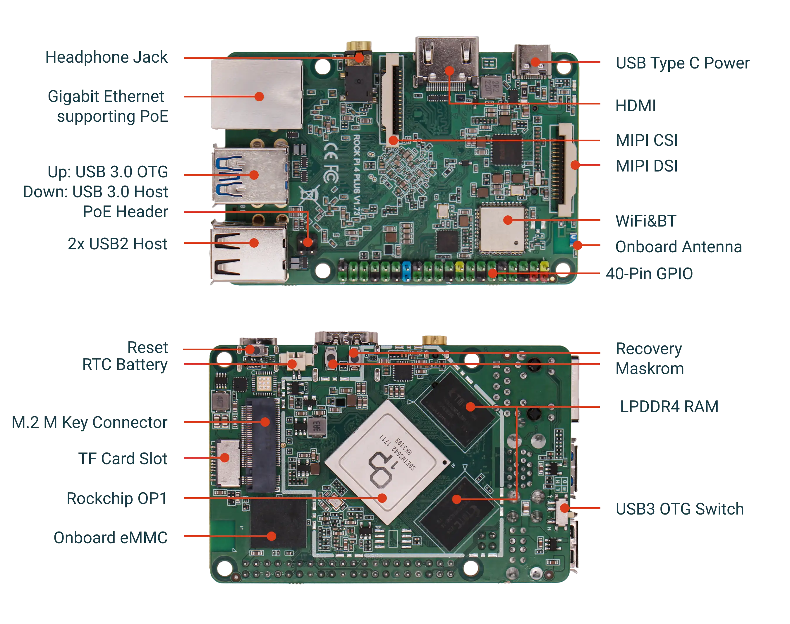
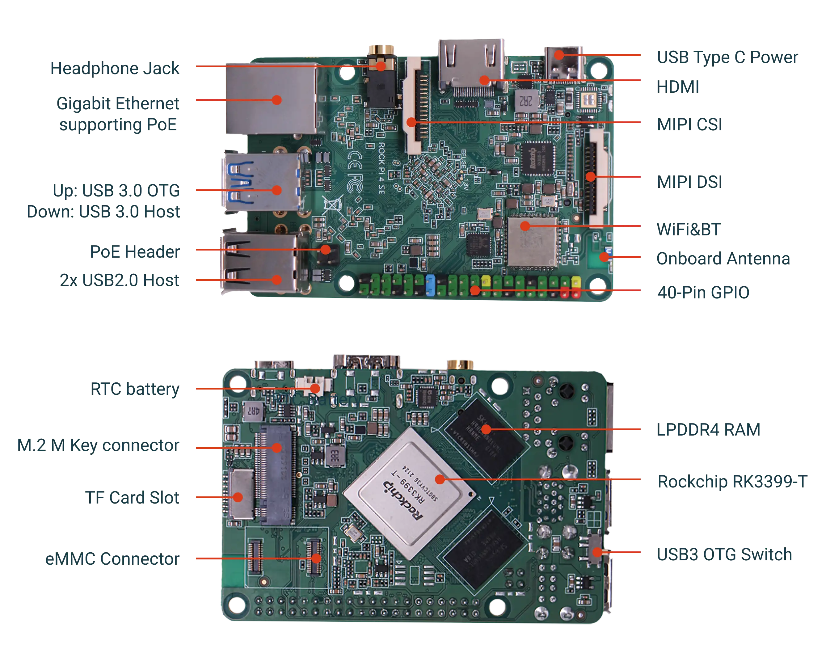
Physical Photos
- ROCK 4A
- ROCK 4B
- ROCK 4A+
- ROCK 4B+
- ROCK 4SE

Interface Specifications
40-PIN GPIO Header
- GPIO Voltage
RK3399 and OP1 have three IO voltage levels: 1.8V/3.0V/3.3V. The following are the default voltages:
| GPIO | Voltage Level | Tolerance |
|---|---|---|
| GPIO3_C0 | 3.3V | 3.465V |
| ADC_IN0 | 1.8V | 1.98V |
| Other GPIO | 3.0V | 3.14V |
- GPIO Interface
The ROCK 4 series features a 40-pin expansion header with color-coded pins, compatible with most sensor applications on the market.
The following pinout applies to all products in the ROCK 4 series.
Not all hardware functions can be enabled simultaneously. At any given time, a pin can only be assigned one hardware function.
| GPIO number | Function2 | Function1 | GPIO | Pin# | Pin# | GPIO | Function1 | Function2 | GPIO number |
|---|---|---|---|---|---|---|---|---|---|
| +3.3V | 1 | 2 | +5.0V | ||||||
| 71 | I2C7_SDA | GPIO2_A7 | 3 | 4 | +5.0V | ||||
| 72 | I2C7_SCL | GPIO2_B0 | 5 | 6 | GND | ||||
| 75 | SPI2_CLK | GPIO2_B3 | 7 | 8 | GPIO4_C4 | UART2_TXD | 148 | ||
| GND | 9 | 10 | GPIO4_C3 | UART2_RXD | 147 | ||||
| 146 | PWM0 | GPIO4_C2 | 11 | 12 | GPIO4_A3 | I2S1_SCLK | 131 | ||
| 150 | PWM1 | GPIO4_C6 | 13 | 14 | GND | ||||
| 149 | SPDIF_TX | GPIO4_C5 | 15 | 16 | GPIO4_D2 | 154 | |||
| +3.3V | 17 | 18 | GPIO4_D4 | 156 | |||||
| 40 | UART4_TXD | SPI1_TXD | GPIO1_B0 | 19 | 20 | GND | |||
| 39 | UART4_RXD | SPI1_RXD | GPIO1_A7 | 21 | 22 | GPIO4_D5 | 157 | ||
| 41 | SPI1_CLK | GPIO1_B1 | 23 | 24 | GPIO1_B2 | SPI1_CSn | 42 | ||
| GND | 25 | 26 | ADC_IN0 | ||||||
| 64 | I2C2_SDA | GPIO2_A0 | 27 | 28 | GPIO2_A1 | I2C2_CLK | 65 | ||
| 74 | I2C6_SCL | SPI2_TXD | GPIO2_B2 | 29 | 30 | GND | |||
| 73 | I2C6_SDA | SPI2_RXD | GPIO2_B1 | 31 | 32 | GPIO3_C0 | SPDIF_TX | UART3_CTSn | 112 |
| 76 | SPI2_CSn | GPIO2_B4 | 33 | 34 | GND | ||||
| 133 | I2S1_LRCK_TX | GPIO4_A5 | 35 | 36 | GPIO4_A4 | I2S1_LRCK_RX | 132 | ||
| 158 | GPIO4_D6 | 37 | 38 | GPIO4_A6 | I2S1_SDI | 134 | |||
| GND | 39 | 40 | GPIO4_A7 | I2S1_SDO | 135 |
-
Notes about the 40-pin header
-
Functions marked in orange are the default functions for those pins.
-
All pins, except for power pins, are directly connected to the SoC.
-
Pins 3, 5, 27, 28, 29, and 31 are each connected to the 3.0V power supply through a 4.7K pull-up resistor.
-
Pin 7 is directly connected to the MIPI CSI pins on the board.
-
SPI
- Pins 19, 21, 23, and 24 are also connected to the SPI flash memory pins on the board. If SPI flash memory is soldered on the ROCK 4 series board, the SPI function will not be available on the GPIO header.
-
UART
-
UART2 is enabled by default as the U-boot and Linux serial console. It can be used by selecting Rockpi4/dev/serial-console. To disable the serial console on UART2, select Rockpi4/hardware/devtree_overlays.
-
UART2 and UART4 support multiple baud rates, including but not limited to: 115200bps, 500000bps, 1500000bps, etc.
-
On some boards with onboard SPI flash memory soldered, the UART4 pins are used for SPI functionality.
-
-
For I2C-2 and I2C-7
- We have tested using an I2C EEPROM device. You need to open the I2C device file first, then perform read or write operations.
-
eMMC Connector
| Pin | Name | Pin | Name |
|---|---|---|---|
| 1 | VCC_1V8 | 2 | VCC3V3_SYS |
| 3 | VCC_1V8 | 4 | VCC3V3_SYS |
| 5 | VCC_1V8 | 6 | VCC3V3_SYS |
| 7 | VCC_1V8 | 8 | VCC3V3_SYS |
| 9 | VCC_1V8 | 10 | GND |
| 11 | GND | 12 | eMMC_RST |
| 13 | GND | 14 | eMMC_CLK |
| 15 | GND | 16 | eMMC_CMD |
| 17 | GND | 18 | eMMC_D7 |
| 19 | GND | 20 | eMMC_D6 |
| 21 | GND | 22 | eMMC_D5 |
| 23 | GND | 24 | eMMC_D4 |
| 25 | GND | 26 | eMMC_D3 |
| 27 | GND | 28 | eMMC_D2 |
| 29 | GND | 30 | eMMC_D1 |
| 31 | GND | 32 | eMMC_D0 |
| 33 | NC | 34 | eMMC_DQS |
| 35 | NC | 36 | NC |
| 37 | NC | 38 | NC |
| 39 | 40 | NC | |
| 41 | 42 | NC |
HDMI
| Pin | Name | Pin | Name |
|---|---|---|---|
| 1 | HDMI_TX2P | 2 | GND |
| 3 | HDMI_TX2N | 4 | HDMI_TX1P |
| 5 | GND | 6 | HDMI_TX1N |
| 7 | HDMI_TX0P | 8 | GND |
| 9 | HDMI_TX0N | 10 | HDMI_TXCP |
| 11 | GND | 12 | HDMI_TXCN |
| 13 | PORT_CEC | 14 | NC |
| 15 | DDC_SCL | 16 | DDC_SDA |
| 17 | GND | 18 | VCC5V0_HDMI |
| 19 | HDMI_HPD | 20 | GND |
| 21 | GND | 22 | GND |
| 23 | GND | 24 |
microSD
| Pin | Name |
|---|---|
| 1 | SDMMC0_D2 |
| 2 | SDMMC0_D3 |
| 3 | SDMMC0_CMD |
| 4 | VCC3V3_SYS |
| 5 | SDMMC0_CLK |
| 6 | GND |
| 7 | SDMMC0_D0 |
| 8 | SDMMC0_D1 |
| 9 | SDMMC0_DET_L |
| 10 | GND |
| 11 | GND |
| 12 | GND |
| 13 | GND |
MIPI CSI
| Pin | Name |
|---|---|
| 1 | VCC_CAM |
| 2 | I2C4_SCL |
| 3 | I2C4_SDA |
| 4 | CAM_MCLK |
| 5 | CAM_GPIO1 |
| 6 | GND |
| 7 | MIPI_RX0_CLKP |
| 8 | MIPI_RX0_CLKN |
| 9 | GND |
| 10 | MIPI_RX0_D1P |
| 11 | MIPI_RX0_D1N |
| 12 | GND |
| 13 | MIPI_RX0_D0P |
| 14 | MIPI_RX0_D0N |
| 15 | GND |
MIPI DSI
| Pin | Name |
|---|---|
| 1 | VCC_MIPI |
| 2 | VCC_MIPI |
| 3 | GND |
| 4 | I2C_SDA_AUDIO |
| 5 | I2C_SCL_AUDIO |
| 6 | GND |
| 7 | MIPI_TX/RX_D0P |
| 8 | MIPI_TX/RX_D0N |
| 9 | GND |
| 10 | MIPI_TX/RX_CLKP |
| 11 | MIPI_TX/RX_CLKN |
| 12 | GND |
| 13 | MIPI_TX/RX_D1P |
| 14 | MIPI_TX/RX_D1N |
| 15 | GND |
PCIe
| Pin | Name | Pin | Name |
|---|---|---|---|
| 1 | GND | 2 | VCC3V3_PCIE |
| 3 | GND | 4 | VCC3V3_PCIE |
| 5 | PCIE_RX3_N | 6 | NC |
| 7 | PCIE_RX3_P | 8 | NC |
| 9 | GND | 10 | NC |
| 11 | PCIE_TX3N | 12 | VCC3V3_PCIE |
| 13 | PCIE_TX3P | 14 | VCC3V3_PCIE |
| 15 | GND | 16 | VCC3V3_PCIE |
| 17 | PCIE_RX2_N | 18 | VCC3V3_PCIE |
| 19 | PCIE_RX2_P | 20 | NC |
| 21 | GND | 22 | NC |
| 23 | PCIE_TX2N | 24 | NC |
| 25 | PCIE_TX2P | 26 | NC |
| 27 | GND | 28 | NC |
| 29 | PCIE_RX1_N | 30 | NC |
| 31 | PCIE_RX1_P | 32 | NC |
| 33 | GND | 34 | NC |
| 35 | PCIE_TX1N | 36 | NC |
| 37 | PCIE_TX1P | 38 | NC |
| 39 | GND | 40 | NC |
| 41 | PCIE_RX0_N | 42 | NC |
| 43 | PCIE_RX0_P | 44 | NC |
| 45 | GND | 46 | NC |
| 47 | PCIE_TX0N | 48 | NC |
| 49 | PCIE_TX0P | 50 | PCIE_PERST_L |
| 51 | GND | 52 | PCIE_CLKREQ_L |
| 53 | PCIE_REF_CLK_N | 54 | NC |
| 55 | PCIE_REF_CLK_P | 56 | NC |
| 57 | GND | 58 | NC |
| 67 | NC | 68 | NC |
| 69 | NC | 70 | VCC3V3_PCIE |
| 71 | GND | 72 | VCC3V3_PCIE |
| 73 | GND | 74 | VCC3V3_PCIE |
| 75 | GND | 76 | GND |
| 77 | GND |
USB
- USB 2.0
| Pin | Name |
|---|---|
| 1 | HOST0_DP |
| 2 | HOST0_DM |
| 3 | TYPEC0_DP |
| 4 | TYPEC0_DM |
| 5 | TYPEC0_ID |
| 6 | TYPEC0_U2VBUSDET |
| 7 | GND |
| 8 | HOST1_DP |
| 9 | HOST1_DM |
| 10 | USB3_DP |
| 11 | USB3_DM |
| 12 | NC |
| 13 | NC |
| 14 | GND |
| 15 | VCC_0V9 |
| 16 | VCCA_1V8 |
| 17 | VCC3V3_SYS |
- USB 3.0
| Pin | Name |
|---|---|
| 1 | USB3_SSTX1P |
| 2 | USB3_SSTX1N |
| 3 | USB3_SSRX1P |
| 4 | USB3_SSRX1N |
| 5 | NC |
| 6 | NC |
| 7 | NC |
| 8 | NC |
| 9 | NC |
| 10 | NC |
| 11 | NC |
| 12 | NC |
| 13 | NC |
| 14 | NC |
| 15 | NC |
| 16 | NC |
| 17 | NC |
| 18 | GND |
| 19 | VCC_0V9 |
| 20 | VCC_0V9 |
| 21 | VCCA_1V8 |
| 22 | VCC3V3_SYS |