Hardware Interface Description
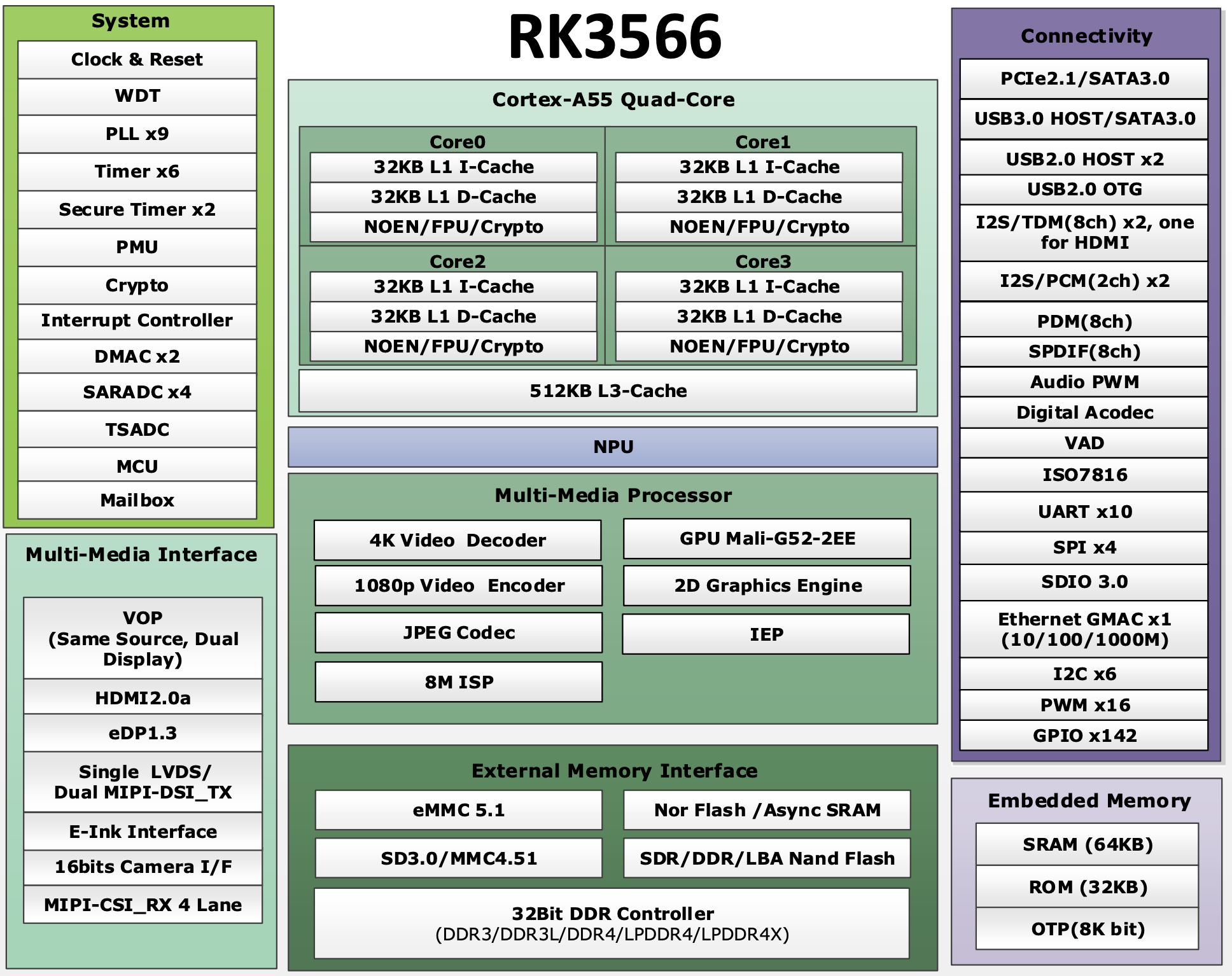
Chip block diagram
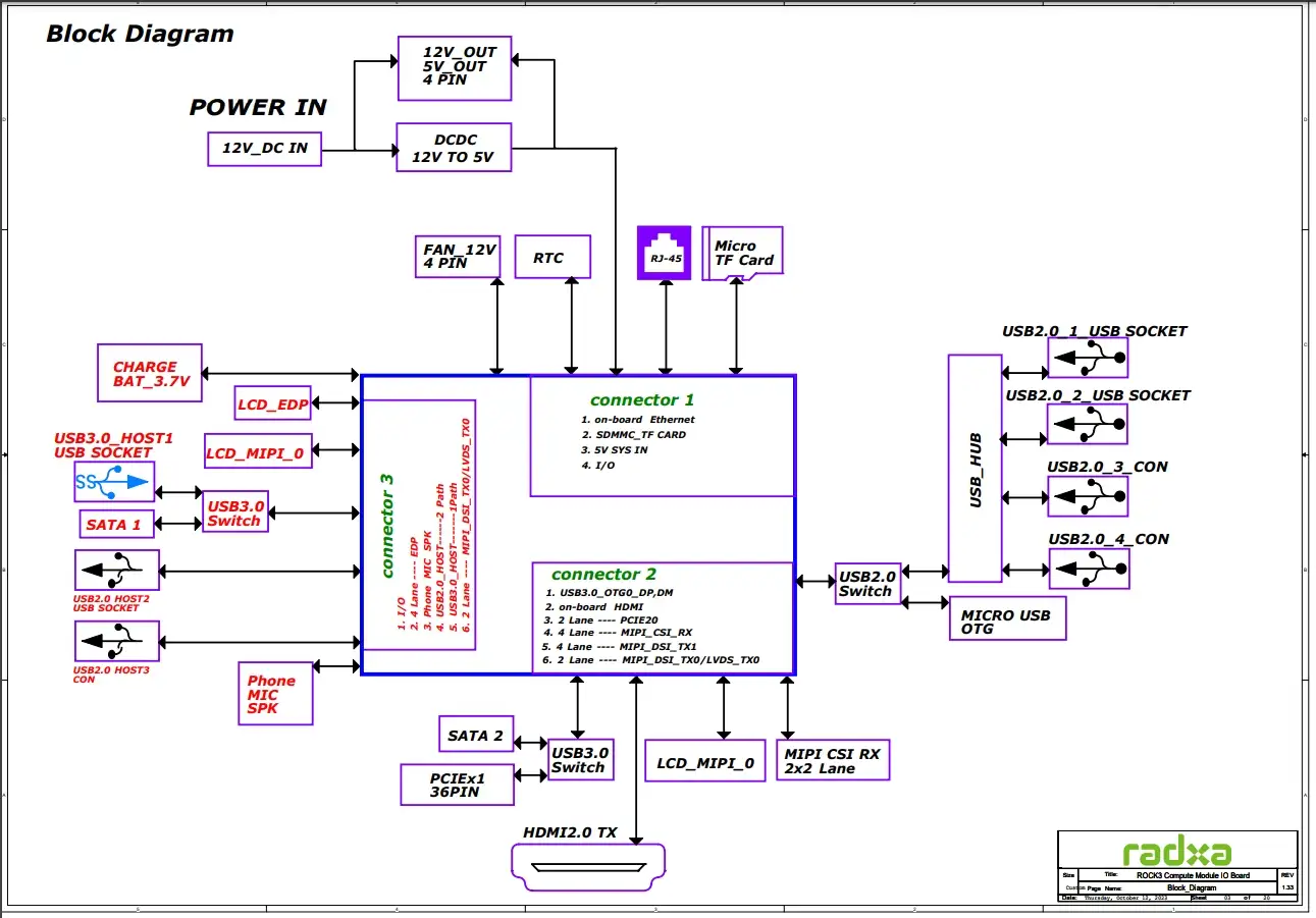
Radxa CM3 IO Board diagram
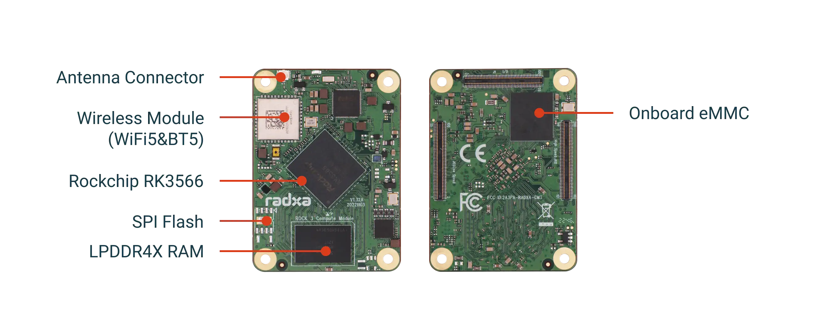
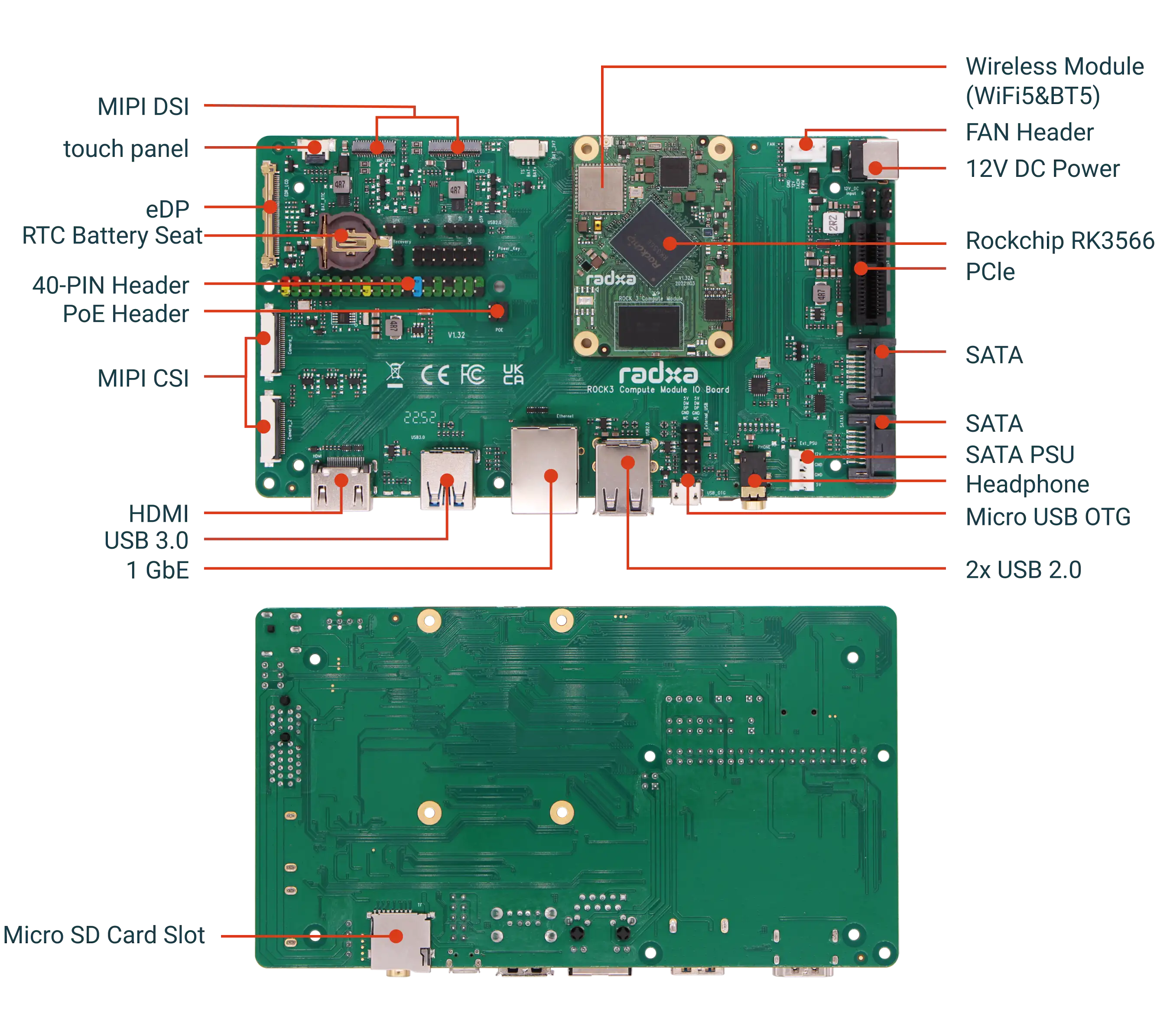
Interface Preview
- CM3 Core Board
- CM3 IO Board
Interface details
The following outlines the comprehensive interface details for the Radxa CM3 IO Board:
BAT
| Pin | Name | Pin | Name |
|---|---|---|---|
| 1 | BAT_3V7_PLUS | 2 | TS |
| 3 | BAT_3V7_LOSE |
DIP_2.54MM_3PIN_180
-
U32
Pin Name Pin Name 1 PWRON_KEY 2 GND 3 RUN_PG
EDP
RK3566 integrates an eDP (Embedded DisplayPort) v1.3 controller, supporting data rates of 1.62Gbps/lane and 2.7Gbps/lane. It operates in 1-lane, 2-lane, and 4-lane modes, with a maximum output resolution of 2560x1600@60Hz. The eDP interface also includes an AUX channel with a maximum rate of 1Mbps.
For the coupled differential signals in the eDP interface, it is recommended to place a 100nF coupling capacitor near the transmitter. It is suggested to use capacitors with 0201 package size to reduce Equivalent Series Resistance (ESR) and Equivalent Series Inductance (ESL).
-
eDP Interface Features:
- Supports 1 eDP 1.3 interface
- Supports up to 4 physical channels of 2.7Gbps
- Supports Panel Self-Refresh (PSR)
- Supports resolutions up to 2560x1600@60Hz
- Supports up to 10-bit RGB format
-
Impedance and Description of eDP Interface Signals:
Signal Impedance Description eDP_TX_DP/DN[3:0] 100ohm±10% eDP TX data transmission, with 100nF capacitor eDP_TX_AUXP/N 100ohm±10% eDP TX auxiliary channel, with 100nF capacitor eDP_HPDIN N/A No eDP TX insertion detection 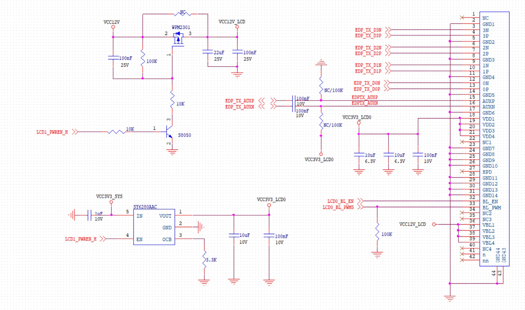
-
eDP Layout Requirements
Range Requirements Trace Impedance 100Ω ±10% differential Max intra‑pair skew <12mil Max trace length on carrier board <6 inches Minimum pair to pair spacing Recommend ≥4 times the width of eDP trace AC coupling capacitors 100nF ±20%, discrete 0201 package preferable Minimum spacing between eDP and other signals ≥4 times the width of eDP trace Maximum allowed via Recommend ≤ 4 vias -
The trace length for the eDP (Embedded DisplayPort) signals on the compute module.
Signal Length EDP_TX_AUXN 1125.784mil EDP_TX_AUXP 1145.200mil EDP_TX_D0N 1,551.442mil EDP_TX_D0P 1,605.627mil EDP_TX_D1N 1,394.502mil EDP_TX_D1P 1,387.683mil EDP_TX_D2N 1,223.146mil EDP_TX_D2P 1,278.783mil EDP_TX_D3N 1,074.909mil EDP_TX_D3P 1,092.072mil Note: On the connector end of the eDP display, it is recommended to reserve a 100k pull-down resistor for AUXP and a 100k pull-up resistor for AUXN.
Ethernet
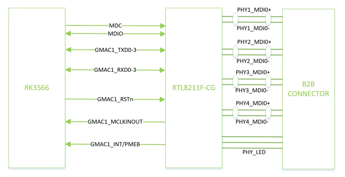
The Radxa CM3 board integrates the Gigabit PHY chip RTL8211F. The four sets of differential signals PHY1_MDI0, PHY1_MDI01, PHY1_MDI02, and PHY1_MDI03 are connected to a B2B connector. When operating at 1000BASE-T, all four sets of differential signals will be utilized. When operating at 100BASE-TX, only PHY1_MDI0 and PHY1_MDI01 will be used.
** Reference Schematic **
** Please refer to the schematic diagram for the specific signal definitions **
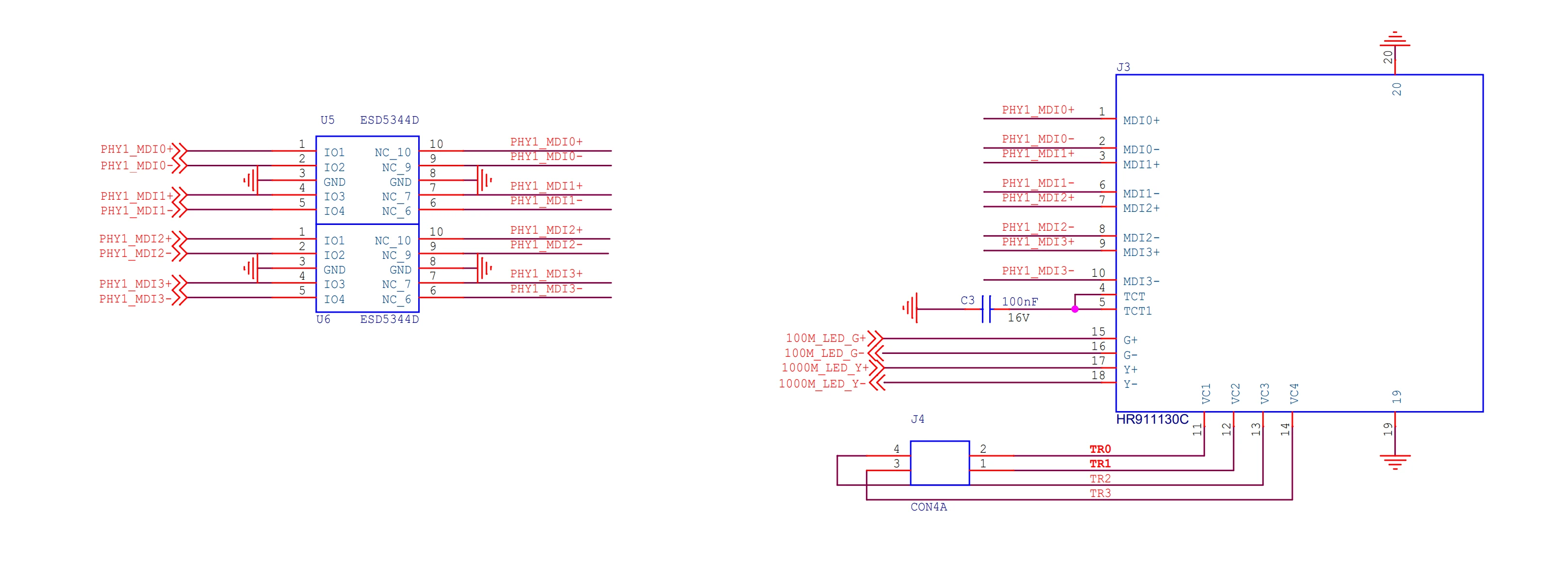
The Radxa CM3 IO Board utilizes an integrated transformer and Ethernet port design. Please refer to the provided design reference as follows:
The trace length for the MDI signals on the compute module.
| Signal | Length |
|---|---|
| PHY1_MDI0+ | 319.903mil |
| PHY1_MDI0- | 326.000mil |
| PHY1_MDI1+ | 249.671mil |
| PHY1_MDI1- | 277.370mil |
| PHY1_MDI2+ | 394.321mil |
| PHY1_MDI2- | 400.440mil |
| PHY1_MDI3+ | 335.779mil |
| PHY1_MDI3- | 347.346mil |
For Gigabit Ethernet, the MDI (Medium Dependent Interface) differential signals are generally controlled to have a differential impedance around 100 ohms.
FAN
| Pin | Name | Pin | Name |
|---|---|---|---|
| 1 | PMW0_M1 | 2 | +5V_INPUT |
| 3 | GND | 4 | GND |
HDMI
HDMI (High-Definition Multimedia Interface) is a unified method of transmitting video and audio data to audio/video display devices through a TMDS (Transition Minimized Differential Signaling) compatible physical link. The HDMI interface is electrically compatible with the DVI (Digital Visual Interface) standard.
-
Features
- HPD (Hot Plug Detect) input analog comparator
- 13.5–600 MHz input reference clock range
- Supports up to 10-bit deep color mode
- Aggregate bandwidth up to 18Gbps
- Supports video resolutions up to 1080p@120Hz and 4096x2304@60Hz
- Compatibility with 3D video formats
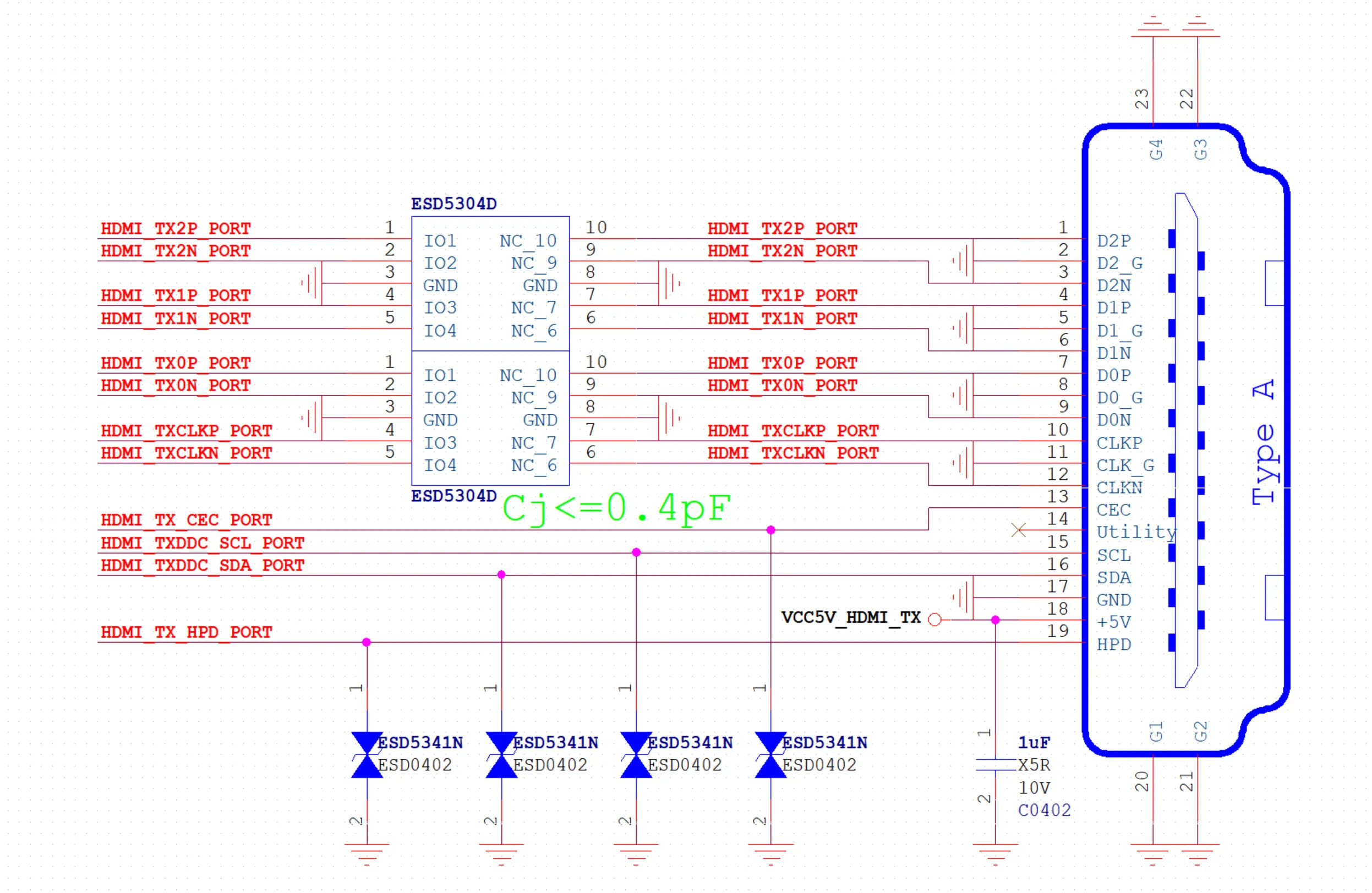
Signal Impedance Description HDMI_TX_DP/DN[2꞉0] 100ohm±10% HDMI TX data transmission HDMI_TX_CLKP/CLKN 100ohm±10% HDMI TX clock transmission HDMI_TX_HPDIN Not specified HDMI TX hot‑plug detection HDMI_TX_REXT Not specified External resistor for HDMI reference connection(Default꞉ 1% precision 1.62k resistor) HDMITX_SCL/SDA Not specified HDMI data communication channel HDMITX_CEC Not specified HDMI Consumer Electronics Control pin On the Radxa CM3 compute module, the HDMITX_SCL/SDA and HDMITX_CEC signals have already gone through level translation processing. The HDMI_TX_HPDIN signal has a 100k ohm pull-down resistor and is connected in series with a 1k ohm resistor to the RK3566. When designing the baseboard, users don't need to worry about level translation issues. Please refer to the following design guide:
-
HDMI 2.0 Layout Requirements
Range Requirements Trace Impedance 100Ω ±10% differential Max intra‑pair skew <12mil Max mismatch between clock and data pairs <480mil Max trace length on carrier board <6 inches Minimum pair to pair spacing ≥5 times the width of HDMI trace (At least 4 times the width of HDMI trace) Minimum spacing between HDMI and other Signals ≥5 times the width of HDMI trace (At least 4 times the width of HDMI trace) Maximum allowed via Recommend ≤ 2 vias -
The trace length for the HDMI signal on the compute module
Signal Length HDMI_TX0N_PORT 1310.556mil HDMI_TX0P_PORT 1302.62mil HDMI_TX1N_PORT 1218.286mil HDMI_TX1P_PORT 1156.647mil HDMI_TX2N_PORT 1122.794mil HDMI_TX2P_PORT 1118.675mil HDMI_TXCLKN_PORT 1437.63mil HDMI_TXCLKP_PORT 1,398.265mil
MIPI CSI
-
Camera_1
Pin Name Pin Name 1 VCC3V3_SYS 2 I2C0_SDA_PMIC 3 I2C0_SCL_PMIC 4 CAM_CLKOUT0 5 CAM_GPIO 6 GND 7 MIPI_CSI_RX_CLK0P 8 MIPI_CSI_RX_CLK0N 9 GND 10 MIPI_CSI_RX_D1P 11 MIPI_CSI_RX_D1N 12 GND 13 MIPI_CSI_RX_D0P 14 MIPI_CSI_RX_D0N 15 GND -
Camera_2
Pin Name Pin Name 1 VCC3V3_SYS 2 I2C2_SDA_M1 3 I2C2_SCL_M1 4 CAM_CLKOUT1 5 CAM_PWR_2 6 GND 7 MIPI_CSI_RX_CLK1P 8 MIPI_CSI_RX_CLK1N 9 GND 10 MIPI_CSI_RX_D3P 11 MIPI_CSI_RX_D3N 12 GND 13 MIPI_CSI_RX_D2P 14 MIPI_CSI_RX_D2N 15 GND
MIPI DSI
-
LCD_1
Pin Name Pin Name 1 VCC_LEDA1 2 VCC_LEDA1 3 VCC_LEDA1 4 GND 5 VCC_LEDK1 6 VCC_LEDK1 7 VCC_LEDK1 8 VCC_LEDK1 9 GND 10 GND 11 MIPI_DSI_TX0_D2P/LVDS_TX0_D2P 12 MIPI_DSI_TX0_D2N/LVDS_TX0_D2N 13 GND 14 MIPI_DSI_TX0_D1P/LVDS_TX0_D1P 15 MIPI_DSI_TX0_D1N/LVDS_TX0_D1N 16 GND 17 MIPI_DSI_TX0_CLKP/LVDS_TX0_CLKP 18 MIPI_DSI_TX0_CLKN/LVDS_TX0_CLKN 19 GND 20 MIPI_DSI_TX0_D0P/LVDS_TX0_D0P 21 MIPI_DSI_TX0_D0N/LVDS_TX0_D0N 22 GND 23 MIPI_DSI_TX0_D3P/LVDS_TX0_D3P 24 MIPI_DSI_TX0_D3N/LVDS_TX0_D3N 25 GND 26 Not Connected 27 MIPI_RESET_1 28 GND 29 VCC_1V8_1 30 VCC_LCD_MIPI 31 VCC_LCD_MIPI -
LCD_2
Pin Name Pin Name 1 VCC_LCD_MIPI_2 2 VCC_1V8_2 3 Not Connected 4 MIPI_RESET_2 5 Not Connected 6 GND 7 MIPI_DSI_TX1_D0N 8 MIPI_DSI_TX1_D0P 9 GND 10 MIPI_DSI_TX1_D1N 11 MIPI_DSI_TX1_D1P 12 GND 13 MIPI_DSI_TX1_CLKN 14 MIPI_DSI_TX1_CLKP 15 GND 16 MIPI_DSI_TX1_D2N 17 MIPI_DSI_TX1_D2P 18 GND 19 MIPI_DSI_TX1_D3N 20 MIPI_DSI_TX1_D3P 21 GND 22 GND 23 TP_RST_LCD 24 VCC_TP 25 TP_INT_LCD 26 I2C2_SDA_LCD 27 I2C2_SCL_LCD 28 GND 29 GND 30 VCC_LCD_MIPI_2 31 VCC_LCD_MIPI_2 32 GND 33 GND 34 VCC_LEDK2 35 VCC_LEDK2 36 Not Connected 37 Not Connected 38 VCC_LEDA2 39 VCC_LEDA2 40 GND 41 VCC_LCD_MIPI_2
PCIe
| Pin | Name | Pin | Name |
|---|---|---|---|
| B1 | VCC12V | A1 | Not Connected |
| B2 | VCC12V | A2 | VCC12V |
| B3 | VCC12V | A3 | VCC12V |
| B4 | GND | A4 | GND |
| B5 | Not Connected | A5 | VCC3V3_PCIE |
| B6 | Not Connected | A6 | VCC3V3_PCIE |
| B7 | GND | A7 | Not Connected |
| B8 | VCC3V3_PCIE | A8 | VCC3V3_PCIE |
| B9 | VCC3V3_PCIE | A9 | VCC3V3_PCIE |
| B10 | VCC3V3_PCIE | A10 | VCC3V3_PCIE |
| B11 | PCIE20_WAKEn | A11 | Pcie_nRST |
| B12 | PCIE20_CLKREQn_M2 | A12 | GND |
| B13 | GND | A13 | PCIE20_REFCLKP |
| B14 | PCIE20_TXP_1 | A14 | PCIE20_REFCLKN |
| B15 | PCIE20_TXN_1 | A15 | GND |
| B16 | GND | A16 | PCIE20_RXP_1 |
| B17 | Not Connected | A17 | PCIE20_RXP_1 |
| B18 | GND | A18 | GND |
| C1 | Not Connected | C2 | Not Connected |
RTC
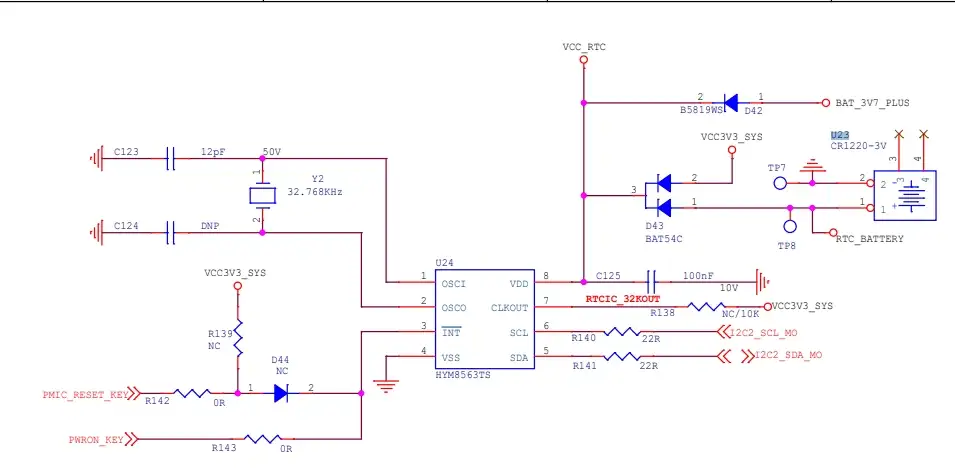
SATA
SATA (Serial Advanced Technology Attachment) is a serial communication hard drive interface supported by RK3566. It supports the SATA 3 protocol and provides the following features:
- Backward compatibility with SATA 1 and SATA 2.
- Supports a maximum data channel signaling rate of 6GT/s.
- Supports Out-of-Band (OOB) communication.
- Supports SATA Power Management (PM) and external chip extension.
- Supports spread spectrum function.
The table below provides the impedance and description of SATA interface signals:
| Signal | Impedance | Description |
|---|---|---|
| SATAx_TXP/N | 90ohm±10% | SATA data transmission, coupling capacitor 10nF placed near the motherboard connector |
| SATAx_RXP/N | 90ohm±10% | SATA data reception, coupling capacitor 10nF placed near the motherboard connector |
SATA 3.0: Consider the following layout requirements
| Parameter | Requirement |
|---|---|
| Line Impedance | 100Ω ±10% differential |
| Maximum intra-pair skew | <1200 ps |
| Maximum trace length on the board | <6 inches |
| AC coupling capacitor | 10nF ±20%, preferably using discrete 0201 package |
| Minimum spacing between pairs | ≥4 times the SATA trace width |
| Minimum spacing from SATA to other signals | ≥4 times the SATA trace width |
| Maximum allowed via count | Recommended ≤ 2 vias |
-
SATA3.0 Port2 J7
Pin Name Pin Name 1 GND 2 SATA1_TXP 3 SATA1_TXN 4 GND 5 SATA1_RXN 6 SATA1_RXP 7 GND 8 GND 9 SATA30_7P_V_DIP -
SATA3.0 Port2 J20
Pin Name Pin Name 1 GND 2 SATA2_TXP 3 SATA2_TXN 4 GND 5 SATA2_RXN 6 SATA2_RXP 7 GND 8 GND 9 SATA30_7P_V_DIP
TP
| Pin | Name | Pin | Name |
|---|---|---|---|
| 1 | TP_RST_L | 2 | VCC3V3_TP |
| 3 | GND | 4 | TP_INT_L |
| 5 | I2C3_SDA_TP | 6 | I2C3_SCL_TP |
| 7 | GND | 8 | GND |
USB
-
USB2.0
Pin Name Pin Name 1 VCC5V0_USB1 2 USB2_DM 3 USB2_DP 4 GND 5 VCC5V0_USB1 6 USB1_DM 7 USB1_DP 8 GND 9 GND 10 GND 11 GND 12 GND -
USB3.0
Pin Name Pin Name 1 5V0_USB30 2 USB3_HOST1_DM 3 USB3_HOST1_DP 4 GND 5 USB3_SSRXN 6 USB3_SSRXP 7 GND 8 USB3_SSTXN 9 USB3_SSTXP 10 GND 11 GND
40-PIN GPIO
- Voltage Range
| Type | Voltage | Tolerance |
|---|---|---|
| GPIO | 3.3V | 3.63V |
| ADC | 1.8V | 1.98V |
- GPIO Interface
Radxa CM3 IO provides a 40 pin GPIO socket, which is compatible with most sensor applications on the market.
Tips: The actual compatibility is subject to usage.
- v1.1
Radxa CM3 IO Board and Raspberry Pi CM4 IO Baseboard's 40-pin expansion header are compatible. The following pinout applies to both products:
| GPIO number | Function4 | Function3 | Function2 | Function1 | Pin# | Pin# | Function1 | Function2 | Function3 | Function4 | GPIO number |
|---|---|---|---|---|---|---|---|---|---|---|---|
| +3.3V | 1 | 2 | +5.0V | ||||||||
| 14 | PWM2_M1 | SPI0_MOSI_M0 | I2C2_SDA_M0 | GPIO0_B6 | 3 | 4 | +5.0V | ||||
| 13 | PWM1_M1 | SPI0_CLK_M0 | I2C2_SCL_M0 | GPIO0_B5 | 5 | 6 | GND | ||||
| 125 | I2S1_SDI3_M1 | GPIO3_D5 | 7 | 8 | GPIO0_D1 | UART2_TX_M0 | 25 | ||||
| GND | 9 | 10 | GPIO0_D0 | UART2_RX_M0 | 24 | ||||||
| 23 | UART0_CTSn | PWM0_M1 | GPIO0_C7 | 11 | 12 | GPIO3_C7 | I2S1_SCLK_TX_M1 | 119 | |||
| 15 | PWM0_M0 | GPIO0_B7 | 13 | 14 | GND | ||||||
| 19 | PWM4 | GPIO0_C3 | 15 | 16 | GPIO3_D4 | I2S1_SDI2_M1 | 124 | ||||
| +3.3V | 17 | 18 | GPIO3_D3 | I2S1_SDI1_M1 | 123 | ||||||
| 138 | I2C4_SDA_M0 | I2S2_SDI_M1 | SPI3_MOSI_M0 | GPIO4_B2 | 19 | 20 | GND | ||||
| 136 | I2S1_SDO1_M1 | SPI3_MISO_M0 | GPIO4_B0 | 21 | 22 | GPIO3_C6 | I2S1_MCLK_M1 | 118 | |||
| 139 | I2C4_SCL_M0 | I2S2_SDO_M1 | SPI3_CLK_M0 | GPIO4_B3 | 23 | 24 | GPIO4_A6 | SPI3_CS0_M0 | I2S1_SCLK_RX | 134 | |
| GND | 25 | 26 | GPIO4_C5 | UART9_TX_M1 | I2S3_SDO_M1 | SPI3_MISO_M1 | |||||
| 140 | I2C2_SDA_M1 | GPIO4_B4 | 27 | 28 | GPIO4_B5 | I2C2_SCL_M1 | I2S1_SDO3_M1 | 141 | |||
| 137 | I2S1_SDO2_M1 | GPIO4_B1 | 29 | 30 | GND | ||||||
| 21 | PWM6 | SPI0_MISO_M0 | GPIO0_C5 | 31 | 32 | GPIO4_C0 | PWM11_IR_M1 | 144 | |||
| 22 | PWM7_IR | SPI0_CS0_M0 | GPIO0_C6 | 33 | 34 | GND | |||||
| 120 | I2S1_LRCK_TX_M1 | GPIO3_D0 | 35 | 36 | GPIO4_A7 | I2S1_LRCK_RX_M1 | 135 | ||||
| 18 | PWM3_IR | GPIO0_C2 | 37 | 38 | GPIO3_D2 | I2S1_SDI0_M1 | 122 | ||||
| GND | 39 | 40 | GPIO3_D1 | I2S1_SDO0_M1 | 121 |
-
More details about 40-pin Header In V1.1
-
Pins marked with color orange are designed for debug console.
-
PWM: x8, PWM0 / PWM1 / PWM2 / PWM3 / PWM4 / PWM6 / PWM7 / PWM11
-
SPI: x2, SPI0 / SPI3
-
I2C: x2, I2C2 / I2C4
-
UART: x1, UART2