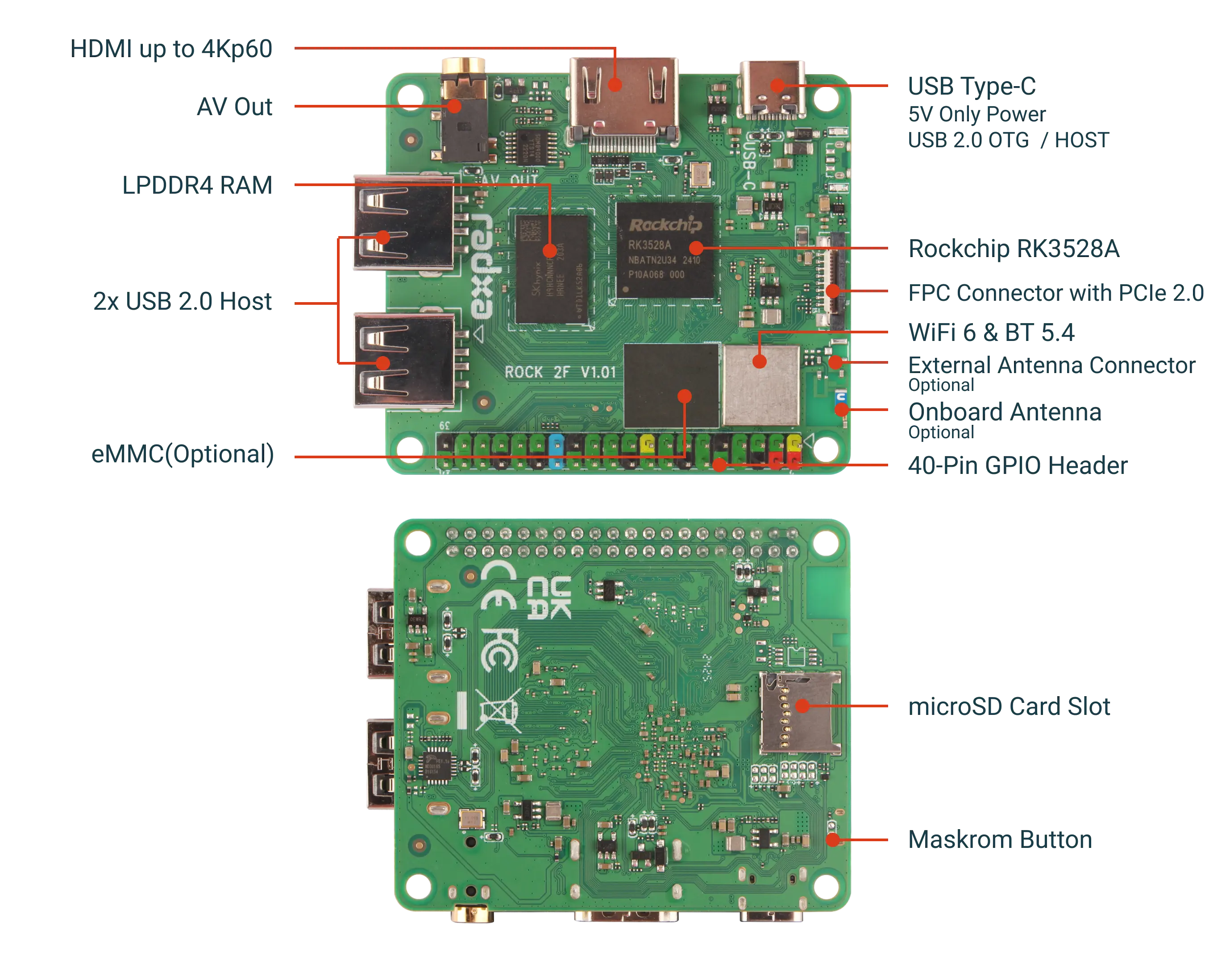
Hardware Overview
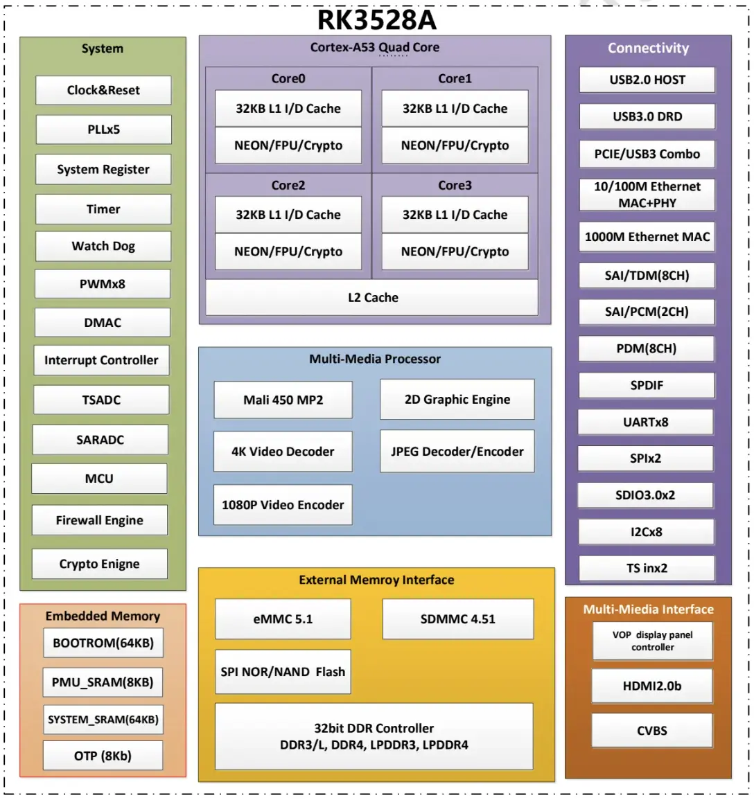
Chip block diagram
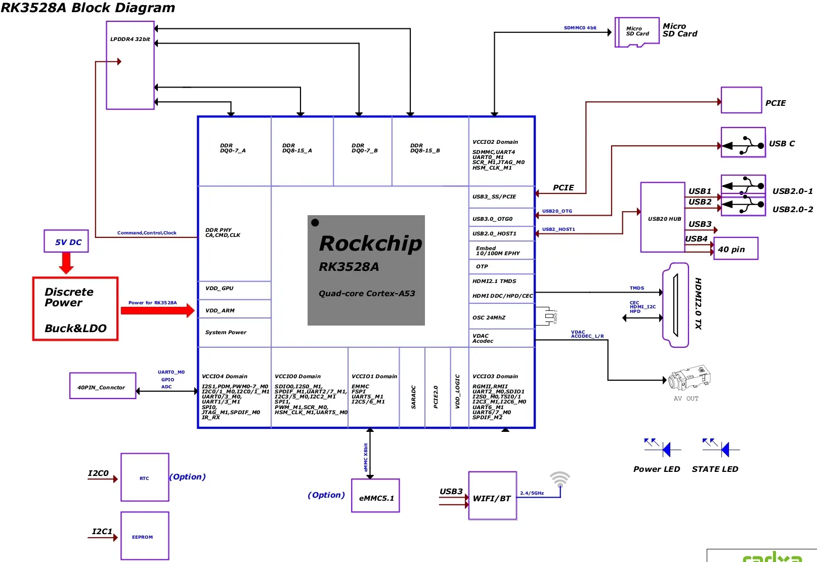
System block diagram
Hardware overview
Below is the detailed interface wiring sequence for each hardware interface.
microSD Card Slot
| PIN | Name |
|---|---|
| 1 | SDMMC_D2 |
| 2 | SDMMC_D3 |
| 3 | SDMMC_CMD |
| 4 | 3V3_SD |
| 5 | SDMMC_CLK |
| 6 | GND |
| 7 | SDMMC_D0 |
| 8 | SDMMC_D1 |
| 9 | SDMMC_DET_L |
| 10 | GND |
HDMI
| Pin | Name | Pin | Name |
|---|---|---|---|
| 1 | HDMI_TX2P_PORT | 2 | GND |
| 3 | HDMI_TX2N_PORT | 4 | HDMI_TX1P_PORT |
| 5 | GND | 6 | HDMI_TX1N_PORT |
| 7 | HDMI_TX0P_PORT | 8 | GND |
| 9 | HDMI_TX0N_PORT | 10 | HDMI_CLKP_PORT |
| 11 | GND | 12 | HDMI_CLKN_PORT |
| 13 | HDMI_TX_CEC_PORT | 14 | X |
| 15 | HDMI_TX_SCL_PORT | 16 | HDMI_TX_SDA_PORT |
| 17 | GND | 18 | VCC5V_HDMI_TX |
| 19 | HDMI_TX_HPD_PORT | 20 | GND |
| 21 | GND | 22 | GND |
| 23 | GND |
WIFI 6 & BT 5.4
| Pin | Name | Pin | Name |
|---|---|---|---|
| 1 | HOST_WAKE_BT_H | 2 | GND |
| 3 | UART1_TX | 4 | GND |
| 5 | GND | 6 | GND |
| 7 | GND | 8 | USB4_DP |
| 9 | USB4_DM | 10 | GND |
| 11 | UART1_RX | 12 | GND |
| 13 | GND | 14 | UART0_RX |
| 15 | UART0_TX | 16 | GND |
| 17 | X | 18 | X |
| 19 | X | 20 | X |
| 21 | X | 22 | X |
| 23 | GND | 24 | VCC_WIFI |
| 25 | GND | 26 | GND |
| 27 | GND | 28 | GND |
| 29 | GND | 30 | X |
| 31 | GND | 32 | X |
| 33 | VCC_WIFI | 34 | VCC_WIFI |
| 35 | GND | 36 | GND |
| 37 | WL_5G_ANT | 38 | WL_24G_ANT |
| 39 | GND | 40 | GND |
| 41 | GND | 42 | GND |
| 43 | GND | 44 | GND |
| 45 | GND | 46 | WIFI_REG_ON_H |
| 47 | WIFI_WAKE_HOST_H | 48 | BT_WAKE_HOST_H |
| 49 | GND | 50 | GND |
| 51 | GND | 52 | GND |
FPC Connector with PCIE 2.0
| Pin | Name | Pin | Name |
|---|---|---|---|
| 1 | VCC5V0_SYS | 2 | VCC5V0_SYS |
| 3 | GND | 4 | PCIE20_REFCLKP |
| 5 | PCIE20_REFCLKN | 6 | GND |
| 7 | USB30_OTG0_SSRXP_PCIE20_RXP | 8 | USB30_OTG0_SSRXN_PCIE20_RXN |
| 9 | GND | 10 | USB30_OTG0_SSTXP_PCIE20_TXP |
| 11 | USB30_OTG0_SSTXN_PCIE20_TXN | 12 | GND |
| 13 | PCIE_EN | 14 | PCIE20_WAKEn_M1 |
| 15 | PCIE20_CLKREQn_M1 | 16 | PCIE20_PERSTn_M1 |
AV Out
| Pin | Name | Pin | Name |
|---|---|---|---|
| 1 | X | 2 | CVBS_OUT |
| 3 | LOUT | 4 | X |
| 5 | GND | 6 | ROUT |
| 7 | X | 8 | X |
2x USB 2.0 HOST
| Pin | Name | Pin | Name |
|---|---|---|---|
| 1 | VCC5V0_USB20 | 2 | USB2_DM |
| 3 | USB2_DP | 4 | GND |
| 5 | GND | 6 | GND |
| Pin | Name | Pin | Name |
|---|---|---|---|
| 1 | VCC5V0_USB20 | 2 | USB3_DM |
| 3 | USB3_DP | 4 | GND |
| 5 | GND | 6 | GND |
40-Pin GPIO Header
GPIO Voltage
| GPIO | Voltage | Max |
|---|---|---|
| All the GPIOs | 3.3V | 3.3V |
| SARADC_IN3 | 1.8V | 1.8V |
GPIO Pinout
The ROCK 2F is supplied with a 40pin pin GPIO Header that is compatible with most sensor applications on the market.
** Actual compatibility is subject to usage. **
- The ROCK 2F has a 40-pin expansion connector. Each pin is color coded.
| GPIO number | Function4 | Function3 | Function2 | Function1 | Pin# | Pin# | Function1 | Function2 | Function3 | Function4 | GPIO number |
|---|---|---|---|---|---|---|---|---|---|---|---|
| +3.3V | 1 | 2 | +5.0V | ||||||||
| 128 | I2C0_SDA_M1 | SPIDIF_TX_M0 | GPIO4_A0 | 3 | 4 | +5.0V | |||||
| 129 | I2C0_SCL_M1 | GPIO4_A1 | 5 | 6 | GND | ||||||
| 134 | UART1_TX_M0 | I2S1_LRCK | GPIO4_A6 | 7 | 8 | GPIO4_D0 | UART2_TX_M0 | 152 | |||
| GND | 9 | 10 | GPIO4_C7 | UART2_RX_M0 | 151 | ||||||
| 143 | PWM4_M0 | UART3_RX_M1 | GPIO4_B7 | 11 | 12 | GPIO1_B5 | I2S0_SCLK_M1 | 45 | |||
| 144 | PWM5_M0 | UART3_TX_M1 | GPIO4_C0 | 13 | 14 | GND | |||||
| 150 | PWM3_M0 | UART1_RX_M1 | I2C1_SDA_M1 | GPIO4_C6 | 15 | 16 | GPIO4_B0 | I2S1_SDO1 | UART3_RX_M0 | 136 | |
| +3.3V | 17 | 18 | GPIO4_B1 | I2S1_SDO2 | PDM_SDI1 | UART3_TX_M0 | 137 | ||||
| 138 | SPI0_MOSI | PDM_SDI0 | I2S1_SDO3 | GPIO4_B2 | 19 | 20 | GND | ||||
| 139 | SPI0_MISO | PDM_SDI2 | I2S1_SDI1 | GPIO4_B3 | 21 | 22 | GPIO1_B2 | UART2_RTSN_M1 | I2C5_SCL_M0 | UART7_TX_M1 | 42 |
| 140 | SPI0_CLK | I2S1_SDI0 | GPIO4_B4 | 23 | 24 | GPIO4_B6 | SPI0_CSN0 | 142 | |||
| GND | 25 | 26 | GPIO4_C1 | PDM_SDI3 | SPI0_CSN1 | PWM6_M0 | 145 | ||||
| 130 | I2C1_SDA_M0 | UART3_RTSN | I2S1_SDI3 | GPIO4_A2 | 27 | 28 | GPIO4_A3 | I2S1_SDI2 | UART3_CTSN | I2C1_SCL_M0 | 131 |
| 141 | PDM_CLK0 | GPIO4_B5 | 29 | 30 | GND | ||||||
| 40 | UART7_CTSN_M1 | UART2_RX_M1 | GPIO1_B0 | 31 | 32 | GPIO4_C3 | I2C0_SDA_M0 | PWM0_M0 | 147 | ||
| 41 | UART7_RTSN_M1 | UART2_TX_M1 | GPIO1_B1 | 33 | 34 | GND | |||||
| 46 | SPI1_CLK | I2S0_LRCK_M1 | GPIO1_B6 | 35 | 36 | GPIO1_B4 | I2S0_MCLK_M1 | 44 | |||
| SARADC_IN3 | 37 | 38 | GPIO1_B7 | I2S0_SDI_M1 | SPI1_MOSI | 47 | |||||
| GND | 39 | 40 | GPIO1_C0 | I2S0_SDO_M1 | SPI1_MISO | 48 |
USB Function Configuration on 40-Pin
On the ROCK 2F's 40-Pin interface, the following pins can be configured for USB 2.0:
- USB1_DM: Pin number 28, resistor location R2417.
- USB1_DP: Pin number 27, resistor location R2416.
By default, Pin-27 can be configured in software for functions such as GPIO4_A2 (see 40-Pin Pinout), while the USB1_DP signal is not activated on the hardware. Pin-28 can be configured in software for functions such as GPIO4_A3 (see 40-Pin Pinout), and the USB1_DM signal is also not activated on the hardware. To change these pins to USB functions, please follow the steps below to modify the reserved resistors:
- Remove the 0-ohm resistors at R2406 and R2407.
- Solder 0-ohm resistors at R2416 and R2417.
The schematic and resistor locations can be viewed and downloaded from the hardware documentation.Hardware Documentation Download
This procedure requires soldering skills, and it is recommended that it be performed by an experienced technician.