Hardware interface description
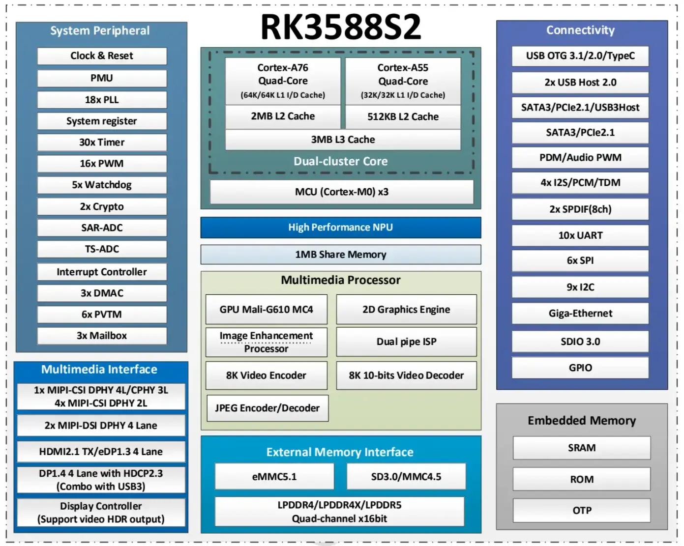
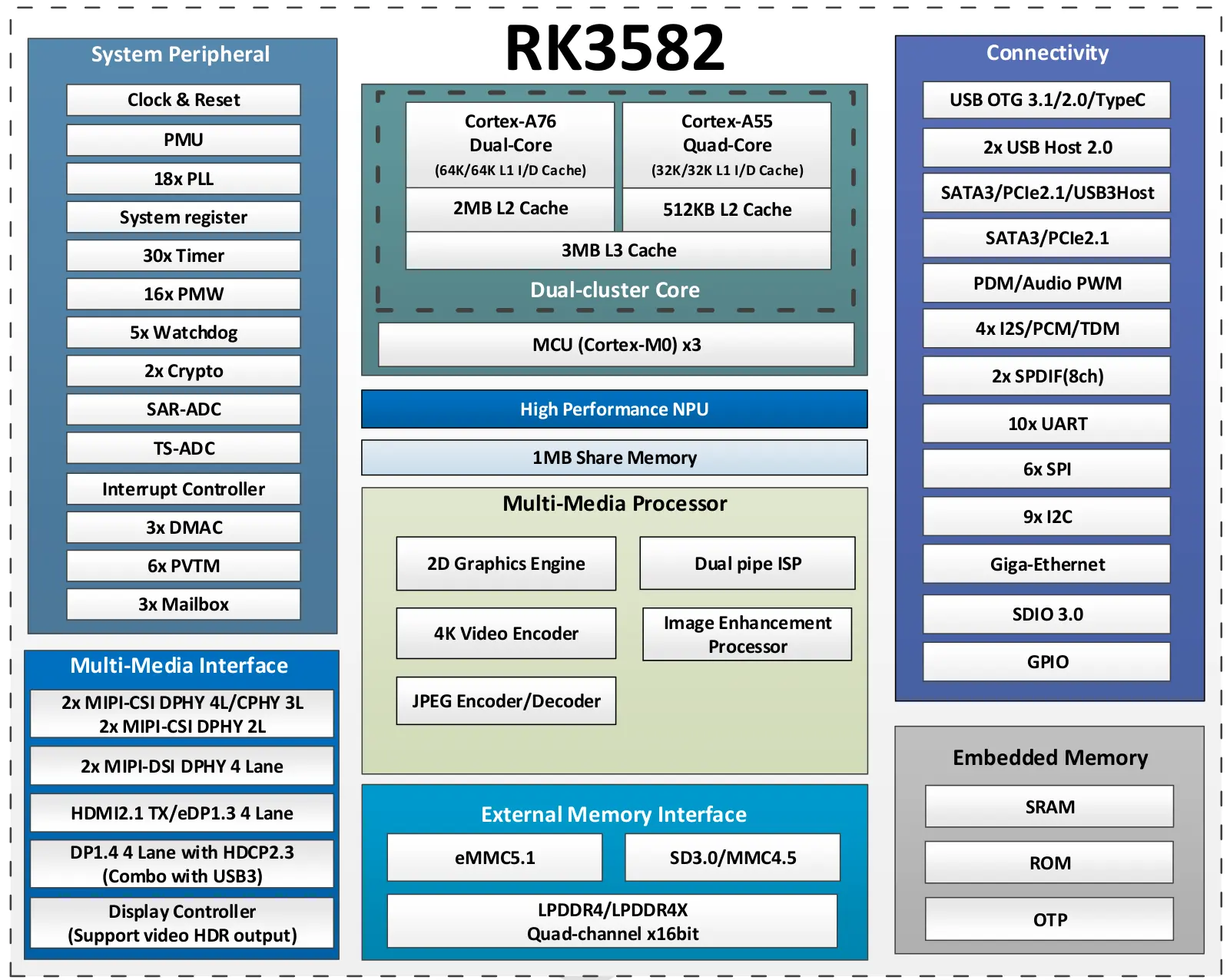
Chip block diagram
- RK3588S2
- RK3582
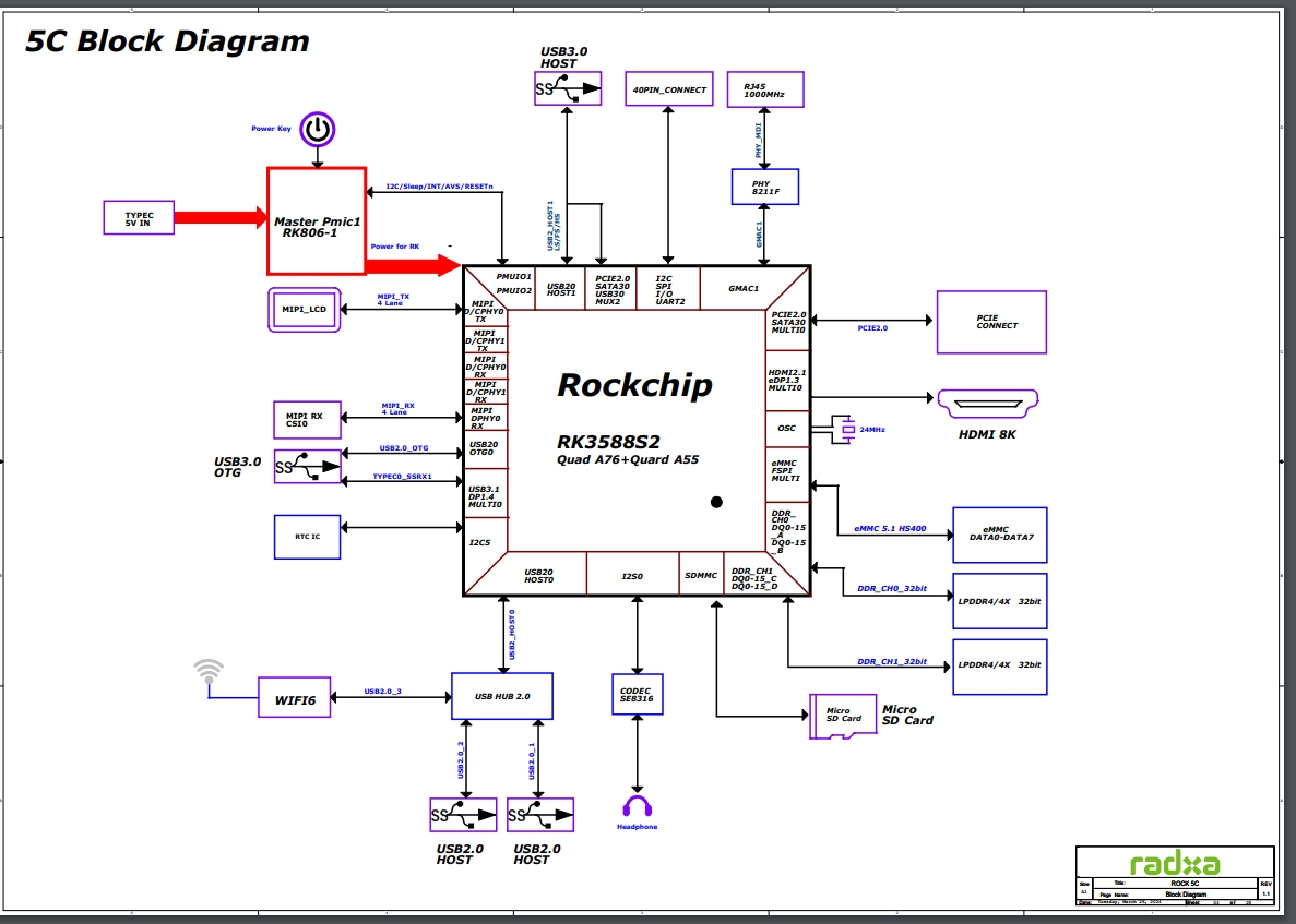
System block diagram
Physical photographs
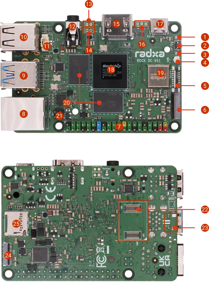
Interface overview
- ROCK 5C
- ROCK 5C Lite
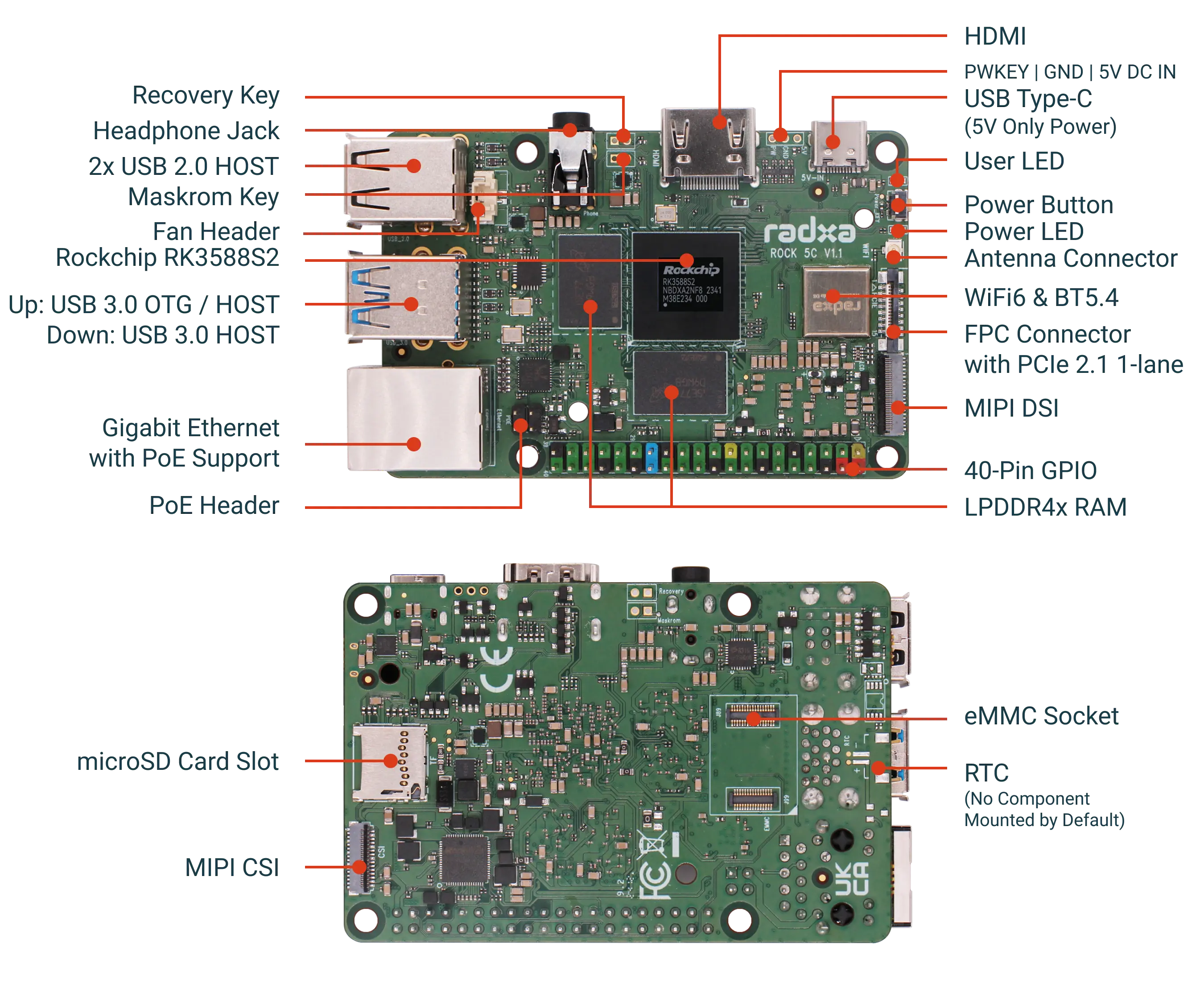
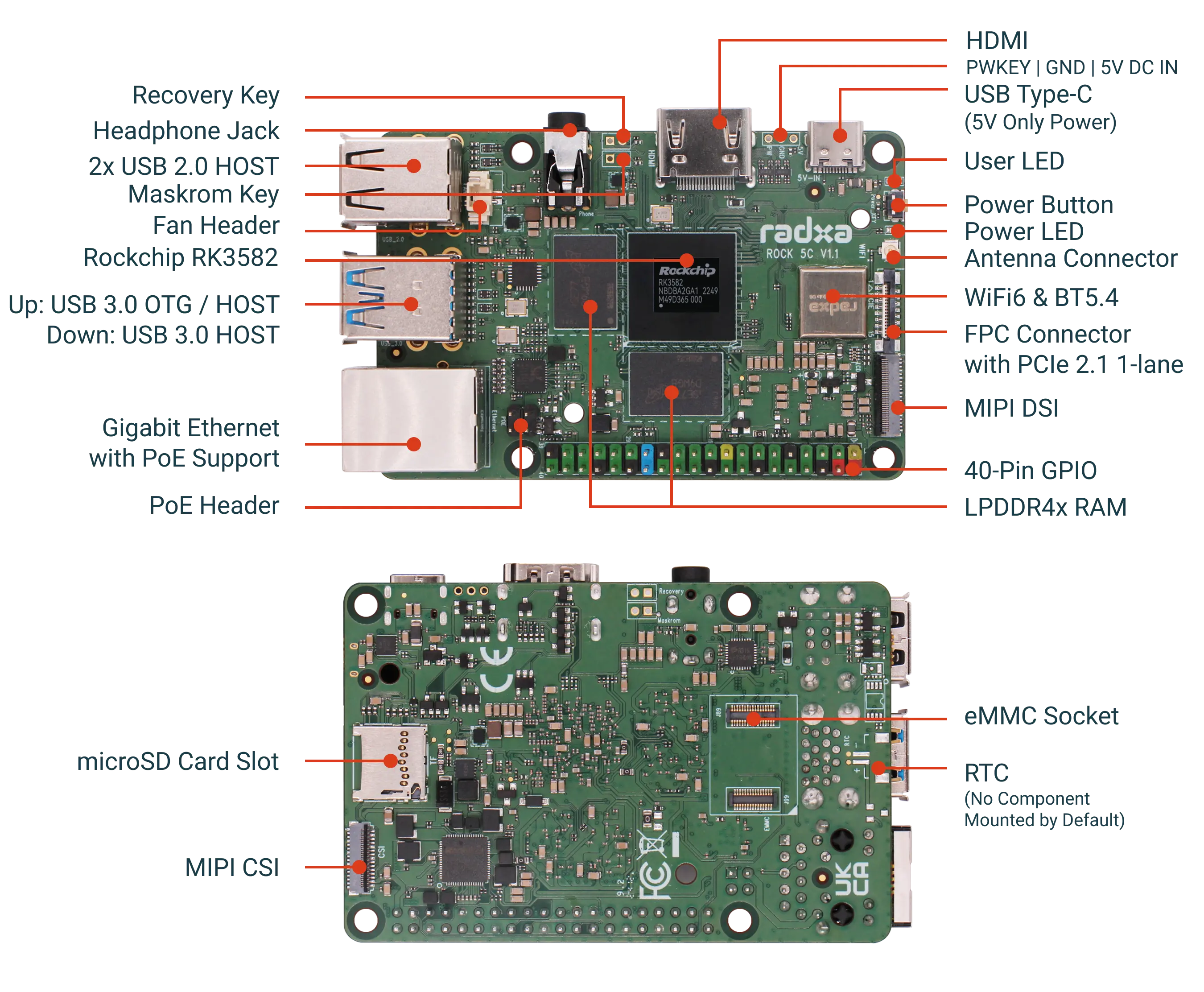
- 1x USB3.0 Host
- 1x USB3.0 OTG
- 2x USB2.0 Host
- 1x 4lane MIPI CSI
- 1x 4lane MIPI DSI
- 1x FPC Pcie 1lane
- 1x TF Card Slot
- 1x Emmc Socket
- 1x Headphone Jack
- 1x HDMI
- 1x Gigabit Ethernet
- 1x 40 PIN IO
- 1x Fan Header
- 2x LED Light
- 1x TypeC Power Input
- 1x Maskrom Key (reserve)
- 1x Recovery Key (reserve)
- 1x Pwrkey/Gnd/5v Header (reserve)
- 1x RTC (reserve)
- 1x Poe Header
- 1x Power Key
Interface details
Power connector
Power adapter with fixed voltage in 5V range on the USB Type-C port
FAN Header
| Pin | Name | Pin | Name |
|---|---|---|---|
| 1 | FAN-PWM | 2 | VCC_5V0 |
| 3 | GND | 4 | GND |
Ethernet Port
Provides Ethernet interface to Gigabit Ethernet.
| Pin | Name | Pin | Name |
|---|---|---|---|
| 1 | PHY1_MDI0+ | 2 | PHY1_MDI0- |
| 3 | PHY1_MDI1+ | 4 | GND |
| 5 | GND | 6 | PHY1_MDI1- |
| 7 | PHY1_MDI2+ | 8 | PHY1_MDI2- |
| 9 | PHY1_MDI3+ | 10 | PHY1_MDI3- |
| 11 | PHY1_MDI0- | 12 | PHY1_MDI0+ |
| 13 | GND | 14 | PHY1_MDI1+ |
| 15 | PHY1_LED_G+ | 16 | PHY1_G_LED- |
| 17 | PHY1_Y_LED+ | 18 | PHY1_Y_LED |
40 PIN GPIO Header
GPIO voltage
| GPIO | Voltage | Max Voltage |
|---|---|---|
| All GPIO | 3.3V | 3.63V |
| SARADC_IN | 1.8V | 1.98V |
GPIO Pinout
ROCK 5C provides a 40pin GPIO socket, which is compatible with most sensor applications on the market. Tips: The actual compatibility is subject to usage.
| GPIO number | Function7 | Function6 | Function5 | Function4 | Function3 | Function2 | Function1 | Pin# | Pin# | Function1 | Function2 | Function3 | Function4 | Function5 | Function6 | Function7 | GPIO number |
|---|---|---|---|---|---|---|---|---|---|---|---|---|---|---|---|---|---|
| +3.3V | 1 | 2 | +5.0V | ||||||||||||||
| 63 | PWM15_IR_M3 | I2C8_SDA_M2 | UART1_CTSN_M1 | GPIO1_D7 | 3 | 4 | +5.0V | ||||||||||
| 62 | PWM14_M2 | I2C8_SCL_M2 | UART1_RTSN_M1 | GPIO1_D6 | 5 | 6 | GND | ||||||||||
| 43 | UART4_TX_M2 | GPIO1_B3 | 7 | 8 | GPIO0_B5 | UART2_TX_M0 | I2C1_SCL_M0 | I2S1_MCLK_M1 | 13 | ||||||||
| GND | 9 | 10 | GPIO0_B6 | UART2_RX_M0 | I2C1_SDA_M0 | I2S1_SCLK_M1 | 14 | ||||||||||
| 139 | I2S1_SDO2_M0 | PWM15_IR_M1 | UART8_CTSN_M0 | GPIO4_B3 | 11 | 12 | GPIO4_A1 | UART9_CTSN_M1 | I2S1_SCLK_M0 | SPI0_MOSI_M1 | 129 | ||||||
| 138 | SPI0_CS0_M1 | I2S1_SDO1_M0 | PWM14_M1 | UART8_RTSN_M0 | GPIO4_B2 | 13 | 14 | GND | |||||||||
| 140 | I2S1_SDO3_M0 | SPDIF0_TX_M1 | PWM11_IR_M1 | UART9_TX_M1 | GPIO4_B4 | 15 | 16 | GPIO1_A5 | SPI2_MOSI_M0 | 37 | |||||||
| +3.3V | 17 | 18 | GPIO1_B0 | SPI2_CS1_M0 | 40 | ||||||||||||
| 33 | SPI4_MOSI_M2 | I2C2_SCL_M4 | UART6_TX_M1 | GPIO1_A1 | 19 | 20 | GND | ||||||||||
| 32 | SPI4_MISO_M2 | I2C2_SDA_M4 | UART6_RX_M1 | GPIO1_A0 | 21 | 22 | GPIO1_B5 | UART7_TX_M2 | SPI0_CS1_M2 | 45 | |||||||
| 34 | SPI4_CLK_M2 | PWM0_M2 | I2C4_SDA_M3 | UART6_RTSN_M1 | GPIO1_A2 | 23 | 24 | GPIO1_A3 | UART6_CTSN_M1 | I2C4_SCL_M3 | PWM1_M2 | SPI4_CS0_M2 | 35 | ||||
| GND | 25 | 26 | GPIO1_A4 | SPI2_MISO_M0 | 36 | ||||||||||||
| 23 | SPI0_MISO_M0 | I2S1_SDI2_M1 | PWM6_M0 | I2C6_SDA_M0 | UART1_RTSN_M2 | GPIO0_C7 | 27 | 28 | GPIO0_D0 | UART1_CTSN_M2 | I2C6_SCL_M0 | PWM7_IR_M0 | I2S1_SDI3_M1 | SPI3_MISO_M2 | 24 | ||
| 42 | SPI0_MOSI_M2 | UART4_RX_M2 | GPIO1_B2 | 29 | 30 | GND | |||||||||||
| 41 | SPI0_MISO_M2 | GPIO1_B1 | 31 | 32 | GPIO4_B0 | UART8_TX_M0 | I2C6_SDA_M3 | I2S1_SDI3_M0 | SPI2_CS1_M1 | 136 | |||||||
| 44 | SPI0_CS0_M2 | UART7_RX_M2 | GPIO1_B4 | 33 | 34 | GND | |||||||||||
| 128 | SPI0_MISO_M1 | I2S1_MCLK_M0 | UART9_RTSN_M1 | GPIO4_A0 | 35 | 36 | GPIO4_A2 | I2S1_LRCK_M0 | SPI0_CLK_M1 | 130 | |||||||
| SARADC_VIN2 | 37 | 38 | GPIO4_A5 | UART3_TX_M2 | I2C3_SDA_M2 | I2S1_SDI0_M0 | 133 | ||||||||||
| GND | 39 | 40 | GPIO4_B1 | UART8_RX_M0 | I2C6_SCL_M3 | SPDIF1_TX_M1 | I2S1_SDO0_M0 | SPI0_CS1_M1 | 137 |
USB Function Configuration on 40-Pin
On the ROCK 5C's 40-Pin interface, the following pins can be configured for USB 2.0:
- USB4_DM: Pin number 28, resistor location R104.
- USB4_DP: Pin number 27, resistor location R106.
By default, Pin-27 can be configured in software for functions such as GPIO0_C7 (see 40-Pin Pinout), while the USB4_DP signal is not activated on the hardware. Pin-28 can be configured in software for functions such as GPIO0_D0 (see 40-Pin Pinout), and the USB4_DM signal is also not activated on the hardware. To change these pins to USB functions, please follow the steps below to modify the reserved resistors:
- Remove the 0-ohm resistors at R169 and R170.
- Solder 0-ohm resistors at R104 and R106.
The schematic and resistor locations can be viewed and downloaded from the hardware documentation.Hardware Documentation Download
This procedure requires soldering skills, and it is recommended that it be performed by an experienced technician.
HDMI
Equipped with a full-size HDMI connector that supports resolutions up to 8K.
USB
Provides two USB3.0 ports and two USB2.0 ports, upper USB3.0 port with OTG function.
- USB2.0
| Pin | Name | Pin | Name |
|---|---|---|---|
| 1 | VCC5V0_USB_HOST | 2 | USB2_HOST1DM |
| 3 | USB2_HOST1DP | 4 | GND |
| 5 | VCC5V0_USB_HOST | 6 | USB2_HOST2DM |
| 7 | USB2_HOST2DP | 8 | GND |
| 9 | GND | 10 | GND |
| 11 | GND |
- USB3.0
| Pin | Name | Pin | Name |
|---|---|---|---|
| 1 | VCC5V0_USB_OTG0 | 2 | USB3_OTG0DM |
| 3 | USB3_OTG0DP | 4 | GND |
| 5 | USB3_OTG0SSRXN | 6 | USB3_OTG0SSRXP |
| 7 | GND | 8 | USB3_OTG0SSTXN |
| 9 | USB3_OTG0SSTXP | 10 | GND |
| 11 | GND | 12 | VCC5V0_USB_HOST |
| 13 | USB3_HOST1DM | 14 | USB3_HOST1DP |
| 15 | GND | 16 | USB3_HOST1SSRXN |
| 17 | USB3_HOST1SSRXP | 18 | GND |
| 19 | USB3_HOST1SSTXN | 20 | USB3_HOST1SSTXP |
| 21 | GND | 22 | GND |
MIPI CSI
MIPI camera support. Utilizes a 31-pin, 0.3 mm pitch, gold-plated connector, model FH35C-31S-0.3SHW(50).
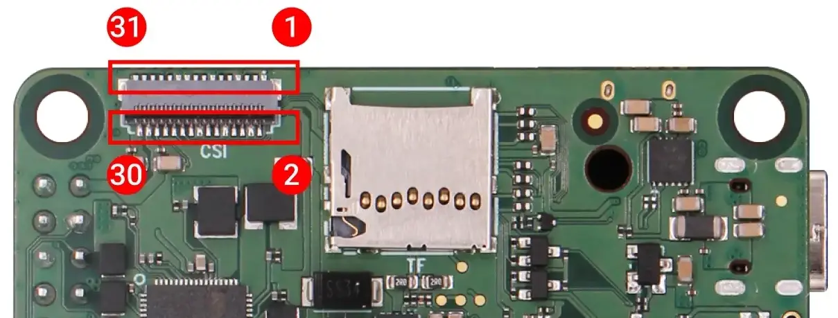
| Number | Pin Name | Voltage | & | Number | Pin Name | Voltage |
|---|---|---|---|---|---|---|
| 1 | GND | & | 2 | CSI_RX_D3N | ||
| 3 | CSI_RX_D3P | & | 4 | GND | ||
| 5 | CSI_RX_D2N | & | 6 | CSI_RX_D2P | ||
| 7 | GND | & | 8 | CSI_RX_CLK1N | ||
| 9 | CSI_RX_CLK1P | & | 10 | GND | ||
| 11 | CSI_RX_D1N | & | 12 | CSI_RX_D1P | ||
| 13 | GND | & | 14 | CSI_RX_D0N | ||
| 15 | CSI_RX_D0P | & | 16 | GND | ||
| 17 | CSI_RX_CLK0N | & | 18 | CSI_RX_CLK0P | ||
| 19 | GND | & | 20 | CAMERA2_CLK | ||
| 21 | GND | & | 22 | CAMERA1_CLK | ||
| 23 | CAM1_PDN_H | 1.8V | & | 24 | SCL_CAM | 1.8V |
| 25 | SDA_CAM | 1.8V | & | 26 | CAM0_PDN_H | 1.8V |
| 27 | CAM_RST | 1.8V | & | 28 | VCC_3V3 | 3.3V |
| 29 | VCC_3V3 | 3.3V | & | 30 | VCC_5V0 | 5V |
| 31 | VCC_5V0 | 5V | & |
Refer Camera accessories
MIPI DSI
MIPI screen support. Utilizes a 39-pin, 0.3 mm pitch, gold-plated connector, model FH35C-39S-0.3SHW(50).
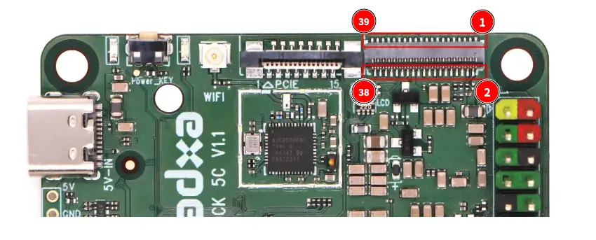
| Number | Pin Name | Voltage | & | Number | Pin Name | Voltage |
|---|---|---|---|---|---|---|
| 1 | VDD3V3 | 3.3V | & | 2 | IOVCC1V8-3V3 | 1.8V |
| 3 | NULL | & | 4 | RESET | 3.3V | |
| 5 | NULL | & | 6 | GND1 | ||
| 7 | MIPI-0N | & | 8 | MIPI-0P | ||
| 9 | GND2 | & | 10 | MIPI-1N | ||
| 11 | MIPI-1P | & | 12 | GND3 | ||
| 13 | MIPI-CKN | & | 14 | MIPI-CKP | ||
| 15 | GND4 | & | 16 | MIPI-2N | ||
| 17 | MIPI-2P | & | 18 | GND5 | ||
| 19 | MIPI-3N | & | 20 | MIPI-3P | ||
| 21 | GND6 | & | 22 | GND7 | ||
| 23 | TP-RESET | 3.3V | & | 24 | TP-VCC | 3.3V |
| 25 | TP-INT | 3.3V | & | 26 | TP-SDA | 3.3V |
| 27 | TP-SCL | 3.3V | & | 28 | GND8 | |
| 29 | GND9 | & | 30 | VCC3V31 | 3.3V | |
| 31 | VCC3V32 | 3.3V | & | 32 | GND11 | |
| 33 | GND12 | & | 34 | LED-1 | ||
| 35 | LED- | & | 36 | NULL | ||
| 37 | NULL | & | 38 | LED+1 | ||
| 39 | LED+ |
Refer Display accessories
microSD
Can be used as a system boot disk or as a storage medium.
| Pin | Name | Pin | Name |
|---|---|---|---|
| 1 | SDMMC_D2 | 2 | SDMMC_D3 |
| 3 | SDMMC_CMD | 4 | VCC_3V3_S3 |
| 5 | SDMMC_CLK | 6 | GND |
| 7 | SDMMC_D0 | 8 | SDMMC_D1 |
| 9 | SDMMC_DET_L | 10 | GND |
| 11 | GND | 12 | GND |
| 13 | GND | 14 | GND |
| 15 | GND | 16 | GND |
| 17 | GND | 18 | GND |
eMMC Socket && SPI Flash Connector
Supports emmc storage devices for use as system boot disks or as storage media.
| Pin | Name | Pin | Name |
|---|---|---|---|
| 1 | GND | 2 | eMMC_D5 |
| 3 | GND | 4 | eMMC_D4 |
| 5 | GND | 6 | eMMC_D0/FSPI_D0 |
| 7 | GND | 8 | eMMC_CLKOUT |
| 9 | GND | 10 | eMMC_D3/FSPI_D3 |
| 11 | GND | 12 | VCCIO_FLASH |
| 13 | GND | 14 | GND |
| 15 | eMMC_DATA_STROBE | 16 | GND |
| 17 | GND | 18 | GND |
| 19 | GND | 20 | GND |
| 21 | GND | 22 | GND |
| 23 | GND | 24 | GND |
| 25 | eMMC_CMD/FSPI_CLK | 26 | GND |
| 27 | eMMC_D2/FSPI_D2 | 28 | GND |
| 29 | eMMC_D1/FSPI_D1 | 30 | GND |
| 31 | eMMC_D7 | 32 | GND |
| 33 | eMMC_D6/FSPI_CS0 | 34 | GND |
| 35 | GND | 36 | GND |
| 37 | GND | 38 | GND |
| 39 | GND | 40 | GND |
| 41 | GND | 42 | GND |
| 43 | GND | 44 | GND |
| 45 | GND | 46 | GND |
| 47 | GND | 48 | GND |
| 49 | GND | 50 | GND |
| 51 | GND | 52 | GND |
| 53 | GND | 54 | GND |
| 55 | GND | 56 | GND |
| 57 | GND | 58 | GND |
| 59 | GND | 60 | GND |
| 61 | GND | 62 | GND |
| 63 | GND | 64 | GND |
eMMC and SPI Flash are mutually exclusive, the connector can only connect to one of eMMC or SPI Flash at a time
Debug Serial Port
For system debugging, underlying log message output