Hardware interface description
Interface overview
-
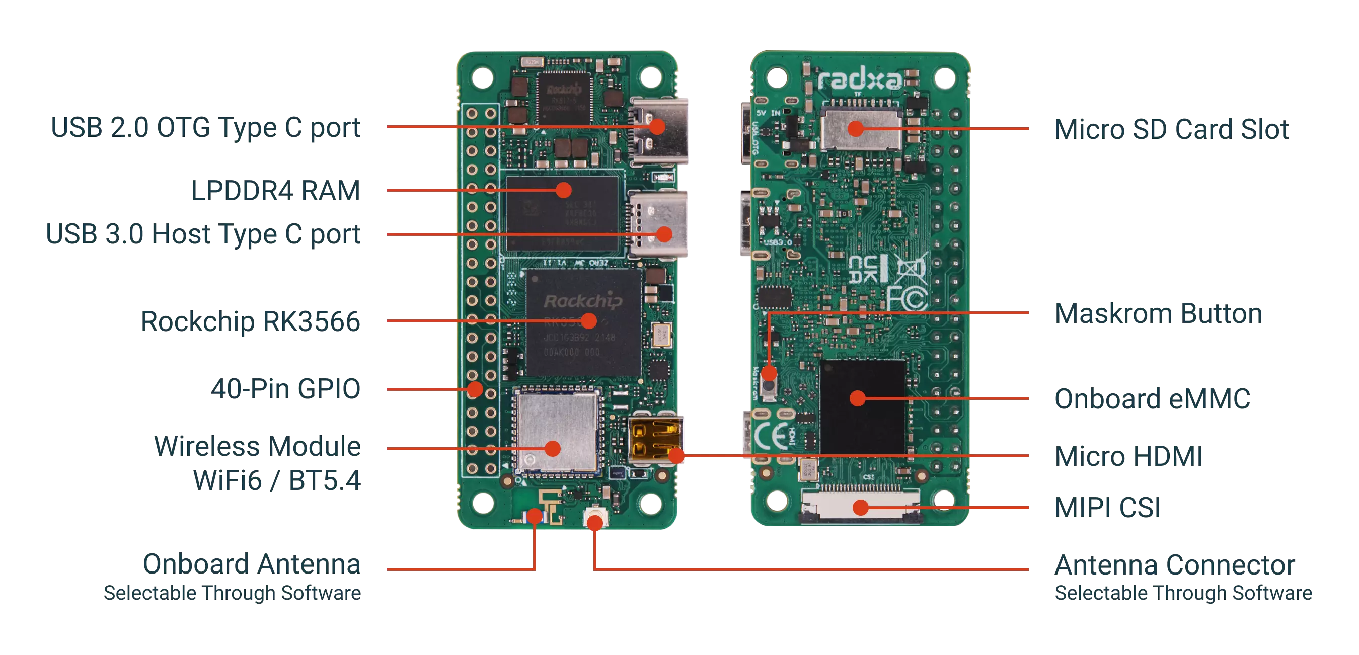
Radxa ZERO 3W
-
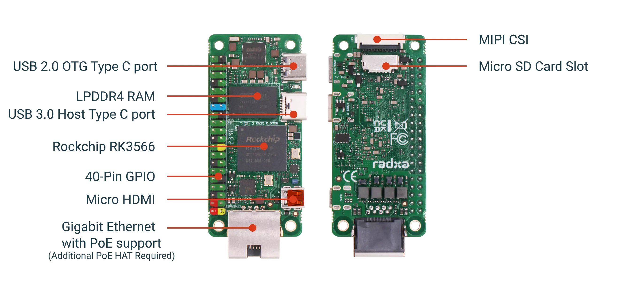
Radxa ZERO 3E
Power
Debug Serial Port
Ethernet Port
40 PIN GPIO
GPIO voltage
| GPIO | Voltage | Maximum |
|---|---|---|
| All GPIOs | 3.3V | 3.63V |
| SARADC_IN5 | 3.3V | 3.3V |
GPIO interface
Radxa ZERO 3 provides a 40-pin GPIO header, which is compatible with most SBC accessories on the market.
Tip: Actual compatibility depends on the use case.
Pin 3, Pin 5, Pin 27, and Pin 28 add extra pull-up resistors for I2C device power supply, so they work abnormally when used as GPIOs.
| GPIO number | Function5 | Function4 | Function3 | Function2 | Function1 | Pin# | Pin# | Function1 | Function2 | Function3 | Function4 | Function5 | GPIO number |
|---|---|---|---|---|---|---|---|---|---|---|---|---|---|
| +3.3V | 1 | 2 | +5.0V | ||||||||||
| 32 | UART3_RX_M0 | GPIO1_A0 | 3 | 4 | +5.0V | ||||||||
| 33 | UART3_TX_M0 | GPIO1_A1 | 5 | 6 | GND | ||||||||
| 116 | PWM14_M0 | GPIO3_C4 | 7 | 8 | GPIO0_D1 | UART2_TX_M0 | 25 | ||||||
| GND | 9 | 10 | GPIO0_D0 | UART2_RX_M0 | 24 | ||||||||
| 97 | GPIO3_A1 | 11 | 12 | GPIO3_A3 | I2S3_SCLK_M0 | 99 | |||||||
| 98 | I2S3_MCLK_M0 | GPIO3_A2 | 13 | 14 | GND | ||||||||
| 104 | GPIO3_B0 | 15 | 16 | GPIO3_B1 | UART4_RX_M1 | PWM8_M0 | 105 | ||||||
| +3.3V | 17 | 18 | GPIO3_B2 | UART4_TX_M1 | PWM9_M0 | 106 | |||||||
| 147 | PWM15_IR_M1 | I2S3_SCLK_M1 | SPI3_MOSI_M1 | GPIO4_C3 | 19 | 20 | GND | ||||||
| 149 | UART9_TX_M1 | PWM12_M1 | I2S3_SDO_M1 | SPI3_MISO_M1 | GPIO4_C5 | 21 | 22 | GPIO3_C1 | I2S1_SDO2_M2 | 113 | |||
| 146 | PWM14_M1 | I2S3_MCLK_M1 | SPI3_CLK_M1 | GPIO4_C2 | 23 | 24 | GPIO4_C6 | SPI3_CS0_M1 | PWM13_M1 | UART9_RX_M1 | I2S3_SDI_M1 | 150 | |
| GND | 25 | 26 | NC | ||||||||||
| 138 | I2C4_SDA_M0 | I2S2_SDI_M1 | GPIO4_B2 | 27 | 28 | GPIO4_B3 | I2C4_SCL_M0 | I2S2_SDO_M1 | 139 | ||||
| 107 | I2C5_SCL_M0 | GPIO3_B3 | 29 | 30 | GND | ||||||||
| 108 | I2C5_SDA_M0 | GPIO3_B4 | 31 | 32 | GPIO3_C2 | UART5_TX_M1 | I2S1_SDO3_M2 | 114 | |||||
| 115 | UART5_RX_M1 | I2S1_SCLK_RX_M2 | GPIO3_C3 | 33 | 34 | GND | |||||||
| 100 | I2S3_LRCK_M0 | GPIO3_A4 | 35 | 36 | GPIO3_A7 | 103 | |||||||
| 36 | I2S1_SCLK_RX_M0 | GPIO1_A4 | 37 | 38 | GPIO3_A6 | I2S3_SDI_M0 | 102 | ||||||
| GND | 39 | 40 | GPIO3_A5 | I2S3_SDO_M0 | 101 |
USB Function Configuration on 40-Pin
On the ZERO 3W / 3E's 40-Pin interface, the following pins can be configured for USB 2.0:
- USB2_HOST2_DM: Pin number 28, resistor location R46.
- USB2_HOST2_DP: Pin number 27, resistor location R45.
By default, Pin-27 can be configured in software for functions such as GPIO4_B2 (see 40-Pin Pinout), while the USB2_HOST2_DP signal is not activated on the hardware. Pin-28 can be configured in software for functions such as GPIO4_B3 (see 40-Pin Pinout), and the USB2_HOST2_DM signal is also not activated on the hardware. To change these pins to USB functions, please follow the steps below to modify the reserved resistors:
- Remove the 0-ohm resistors at R32 and R39.
- Solder 0-ohm resistors at R45 and R46.
The schematic and resistor locations can be viewed and downloaded from the hardware documentation.Hardware Documentation Download
This procedure requires soldering skills, and it is recommended that it be performed by an experienced technician.
USB C
There are two USB TYPE-C ports, one is USB 2.0 OTG port and the other is USB3.0 HOST port. The power supply is USB 2.0 OTG port.
HDMI
Provides a Micro HDMI port.
MIPI CSI
| PIN | Name |
|---|---|
| 1 | GND |
| 2 | MIPI_CSI_RX_D0N |
| 3 | MIPI_CSI_RX_D0P |
| 4 | GND |
| 5 | MIPI_CSI_RX_D1N |
| 6 | MIPI_CSI_RX_D1P |
| 7 | GND |
| 8 | MIPI_CSI_RX_CLK0N |
| 9 | MIPI_CSI_RX_CLK0P |
| 10 | GND |
| 11 | MIPI_CSI_RX_D2N |
| 12 | MIPI_CSI_RX_D2P |
| 13 | GND |
| 14 | MIPI_CSI_RX_D3N |
| 15 | MIPI_CSI_RX_D3P |
| 16 | GND |
| 17 | CAMERAB_PDN_L |
| 18 | CIF_CLKOUT |
| 19 | GND |
| 20 | I2C2_SCL_M1 |
| 21 | I2C2_SDA_M1 |
| 22 | VCC_3V3 |